You will not see much instability with 22R because then the current components of the cap is not dominant.
But then a real headphone + cable will probably not be 47n either.
The easy way round is to limit the bandwidth in the feedback network.
Alternative is output Zobel.
But they will also change if you change the MOSFETs.
So maybe limit bandwidth for now and decide on the MOSFETs first.
Patrick
But then a real headphone + cable will probably not be 47n either.
The easy way round is to limit the bandwidth in the feedback network.
Alternative is output Zobel.
But they will also change if you change the MOSFETs.
So maybe limit bandwidth for now and decide on the MOSFETs first.
Patrick
Thank you for sparing me the indignity of having to think ")
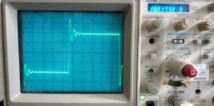
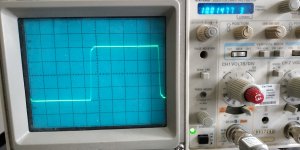
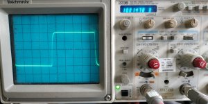
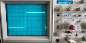
Here's with 2x100p compensation, and 22R+100nF Zobel, with different loads:
Here's with 2x100p compensation, and 22R+100nF Zobel, with different loads:
- 300R//47nF: ringing almost gone
- 300R//10nF:definitely gone
- 300R//100nF: ringing back
Attachments
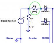
It appears to me that (i) there is a LOT of reservoir capacitance; (ii) the in-to-out voltage across the regulator ICs, far exceeds their dropout spec.
Together, these may suggest there is plenty of excess headroom, and some of it can be safely traded away in exchange for other benefits. One possibility is to insert current limiting resistors ("R9") between the secondary and the rectifier bridge.
These resistors reduce the magnitude of the peak diode current (and the peak capacitor current), which in this simulation is around 2 amperes. Setting ".PARAM xxx=2.0" ohms, for example, reduces the current peak to 1 ampere and also reduces the diode's peak instantaneous power dissipation by more than 3x.
Reducing the diode peak current reduces the magnetic field generated by the secondary + rectifiers current loop, which reduces the amount of HF "hash" broadcasted throughout the chassis. It also reduces the magnitude of the diode turn-off event, which reduces the stimulus applied to the RLC resonant circuit containing the leakage inductance of the secondary. Smaller stimulus ---> smaller ringing amplitude, if your ringing-snubber's damping ratio zeta isn't set correctly.
Reducing diode peak current also places less stress on the transformer and on the mains fuse, in case either of them is uncomfortably scrawny. Perhaps a pancake flat transformer from Talema is the only thing which fits in your slimline chassis, and perhaps its VA rating is not enormously greater than the circuit's requirements.
Finally, inserting R9 gives a first stage of lowpass filtering to reduce RFI. R9-C11 have a roll-off corner of 0.8 MHz, which is a good start towards reducing HF noise that the regulator ICs would otherwise happily pass thru with no attenuation whatsoever.
Naturally the thing to do in design is to .STEP the value of R9 across a broad range, and choose whichever value gives simulated results that please you most. I believe/imagine/suspect that your final choice will probably NOT be R9=Zero.
_
Attachments
Last edited:
So much fun.
Patrick
Oh, and they keep coming: I just blew up my Valhalla, the PS board for my Linn LP12. There goes my plan B for my 1st item in the backlog.
It appears to me that (i) there is a LOT of reservoir capacitance; (ii) the in-to-out voltage across the regulator ICs, far exceeds their dropout spec.
Together, these may suggest there is plenty of excess headroom, and some of it can be safely traded away in exchange for other benefits. One possibility is to insert current limiting resistors ("R9") between the secondary and the rectifier bridge.
_
Good points, Mark.
- there is a LOT of reservoir capacitance.
This is actually by design: if I were to use a passive PS, I would specify 10,000uF or more; here, I wanted to see if there could be some sort of compromise: 1/5 of what I would use, but with a not-so-fancy regulator behind, plus a cap multiplier after. Your view is based on good engineering practice, mine is more related to black magic. - the in-to-out voltage across the regulator ICs, far exceeds their dropout spec.
This is because I didn't know what I was doing in the beginning (and still now): for reasons long forgotten, I wanted 16V to the amp, and getting that from a standard 15V winding is cutting it a bit too close, so 18Vac it is. In practice, the delta temp. is quite reasonable. - One possibility is to insert current limiting resistors
That would totally negate the voodoo listed under 1.: "Thou shall use as stiff a PS as possible"
Btw, the Chinese R-Core trafos work wonderful in spite of my barbarous treatment, and the peak current in both the diodes and the caps is more like 3.5A, so said LTspice.
Look at the ripple waveform at the input to the voltage regulator IC. It has gotten slightly smaller (in peak-to-peak magnitude). Your big cap-to-ground with its very low impedance at 100Hz, has not changed. The impedance is still low. What has changed is: the cap's opponent, against whom it fights. Now the puller-upper mechanism, which creates the rising edges of the ripple sawtooth waveform, is not quite as strong as it used to be. So the rising edges are less steep and they rise up to a slightly lower tippy top. None of this is bad.
In the frequency domain, these are very good arguments indeed; the lower ripple is due to the reduction in Fo in the low-pass.
In the time domain, with a current sink driven by a pulse, the difference is a bit larger, again, totally normal because of the charging time.
But still, I wouldn't throw away my low Z PS in exchange of a degree or so of reduction in temperature, no way.
Edit
On 2nd thought, the box temp remains more or less the same: the regulator cools a bit, the additional R heats a bit, we're even
Last edited:
- Home
- Amplifiers
- Headphone Systems
- The JC2-HPA Headphone Amplifier