Hello guys,
About half a year ago I decided to design my own high performance headphone amplifier. The idea came more from some kind of engineering challenge rather than serious need - my O2 was probably more than enough.
My designs considerations were pretty simple:
Finally I decided to nest already very good TPA6120A2 inside feedback loop of another operational amplifier. At this time I'm using OPA1602 but want to experiment with something else like OPA1652 or OPA1656. Especially the last one seems promising but first I need better test equipment to analyze such small distortion levels.
TPA6120A2 is almost perfect candidate apart from one thing - stability. It is current feedback operational amplifier and its stability is not so easy to tame. High attention must be paid to minimize stray capacitances at PCB.
Apart from that TI recommends at least 10 ohms of series output resistance. But this means rather high output impedance. I tried to address this issue in two ways - complex feedback, post output resistor or output inductor.
At this time I'm using ~300nH air core inductor at output. TPA6120A2 seems happy with it and output impedance is very low, about 10 miliohms. There is downside tho. Such inductors are hard to get off the shelf so I had to hand wound them. Inductors with other that air cores probably would introduce high distortions.
But there is another way. PCB can be configured to take feedback post resistor/inductor. This configuration is not so popular way of isolating capacitive load from amplifier while maintaining low output impedance. I haven't tried it yet but possibility of omitting inductor is very promising.
For power supply good, old LM317 and LM337 regulators are used with half wave rectifier. Board can be powered by AC-AC wall wart or transformer. Those wall warts are cheap and easy to use as there is no contact with potentially dangerous mains wiring.
Instead of using more common voltage divider to set output voltage I decided to use zener diodes. Dynamic resistance of zener diode is lower than required resistor which should result in lower output noise. By default 13V zeners yields about +/- 14.5V at output with less than 10mV difference between negative and positive rails.
Cadj capacitors are of course present. There are two LEDs at both rails. Besides being indicators they run at relatively high current, providing constant load to regulators which keeps low output impedance of power supply.
Whole PCB was designed in free and open source software - KiCad. Simulations were done in LTspice.
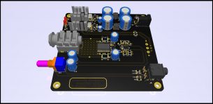
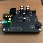
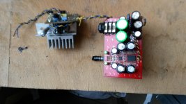
3D render, real photo taken before mounting my ugly hand wound inductors and schematics could be found in attachment.
What are my plans for future?
About half a year ago I decided to design my own high performance headphone amplifier. The idea came more from some kind of engineering challenge rather than serious need - my O2 was probably more than enough.
My designs considerations were pretty simple:
- Challenge myself and check what lowest distortion can I archive
- Decent power with ability to drive almost any headphones
- Near zero output impedance
- Safe for headphones, no DC at output and stability in any conditions
- Relatively cheap and easy to build - no unobtainable, expensive or exotic parts
Finally I decided to nest already very good TPA6120A2 inside feedback loop of another operational amplifier. At this time I'm using OPA1602 but want to experiment with something else like OPA1652 or OPA1656. Especially the last one seems promising but first I need better test equipment to analyze such small distortion levels.
TPA6120A2 is almost perfect candidate apart from one thing - stability. It is current feedback operational amplifier and its stability is not so easy to tame. High attention must be paid to minimize stray capacitances at PCB.
Apart from that TI recommends at least 10 ohms of series output resistance. But this means rather high output impedance. I tried to address this issue in two ways - complex feedback, post output resistor or output inductor.
At this time I'm using ~300nH air core inductor at output. TPA6120A2 seems happy with it and output impedance is very low, about 10 miliohms. There is downside tho. Such inductors are hard to get off the shelf so I had to hand wound them. Inductors with other that air cores probably would introduce high distortions.
But there is another way. PCB can be configured to take feedback post resistor/inductor. This configuration is not so popular way of isolating capacitive load from amplifier while maintaining low output impedance. I haven't tried it yet but possibility of omitting inductor is very promising.
For power supply good, old LM317 and LM337 regulators are used with half wave rectifier. Board can be powered by AC-AC wall wart or transformer. Those wall warts are cheap and easy to use as there is no contact with potentially dangerous mains wiring.
Instead of using more common voltage divider to set output voltage I decided to use zener diodes. Dynamic resistance of zener diode is lower than required resistor which should result in lower output noise. By default 13V zeners yields about +/- 14.5V at output with less than 10mV difference between negative and positive rails.
Cadj capacitors are of course present. There are two LEDs at both rails. Besides being indicators they run at relatively high current, providing constant load to regulators which keeps low output impedance of power supply.
Whole PCB was designed in free and open source software - KiCad. Simulations were done in LTspice.
3D render, real photo taken before mounting my ugly hand wound inductors and schematics could be found in attachment.
What are my plans for future?
- Learn CAD software to design enclosure and order it at CNC workshop
- Acquire/build equipment allowing me to measure true performance of amplifier (aiming <-130 dB THD)
- Adding micro controller (probably STM32) used for monitoring amplifier - temperatures, DC offset, failure, relay control and etc.
- Maybe bigger version with XLR input, preamp output, switchable gain and Alps RK27 volume control?
Attachments
Everything was measured with Audio Precision APx525. Unless otherwise noted given conditions were used: 1kHz, 2Vrms, 150Ω load, AC - 20kHz bandwidth, no weighting, maximum power at 1% THD+N, both channels driven.
Gain: 12dB (x4)
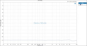
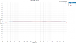
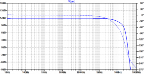
Frequency response (±0.1dB): 12Hz – >80kHz
20Hz – 20kHz ±0.05 dB
Output impedance: <10mΩ
DC offest: <300µV
THD+N 1kHz: <-110dB
THD 1kHz: <-117dB
SNR: >124dB
Power, 32Ω: 3W per channel
Power, 150Ω: 700mW per channel
Power, 600Ω: 185mW per channel
As you can see I'm limited by performance of Audio Precision APx525. Unfortunately I don't have analog oscillator option installed in my AP so SINAD measurements are limited to about 105-110dB. Measurements were done without any enclosure in very noisy lab with cheap cables.
Gain: 12dB (x4)
Frequency response (±0.1dB): 12Hz – >80kHz
20Hz – 20kHz ±0.05 dB
Output impedance: <10mΩ
DC offest: <300µV
THD+N 1kHz: <-110dB
THD 1kHz: <-117dB
SNR: >124dB
Power, 32Ω: 3W per channel
Power, 150Ω: 700mW per channel
Power, 600Ω: 185mW per channel
As you can see I'm limited by performance of Audio Precision APx525. Unfortunately I don't have analog oscillator option installed in my AP so SINAD measurements are limited to about 105-110dB. Measurements were done without any enclosure in very noisy lab with cheap cables.
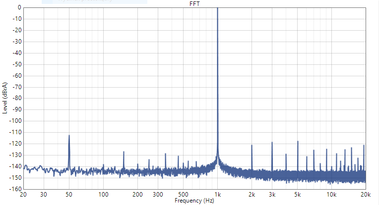
FFT 1kHz, 256k length, 8x avg.
Everything looks same like direct APx525 loopback, maybe apart from 50Hz peak coming from mains. Lab in which tests were performed is very noisy.
Frequency response
There is low pass and high pass filters at input of amp for filtering out possible DC voltage or radio frequency intererences.
APx525 is limited to only 80kHz. I also have access to Audio Precision System Two with higher bandwidth but I think such high frequencies are not meaningful anyway.
Note the scale used - 1dB max with 0.1dB step.

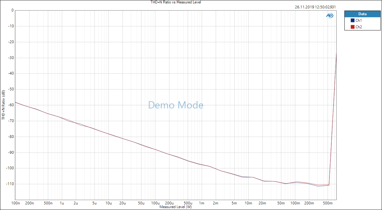
THD+N 1kHz vs measured power with 150Ω load
THD 1kHz vs measured power with 150Ω load
Measurement similar to previous one but only harmonic products, excluding noise

THD+N 1kHz vs measured power with 32Ω load

and for comparison
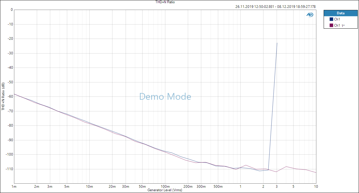
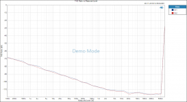
THD+N 1kHz vs level - blue channel is amplifier and red is Audio Precision loopback
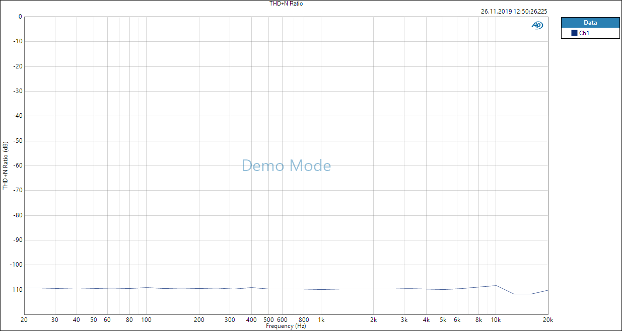
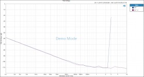
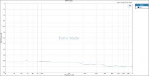
THD+N ratio vs frequency
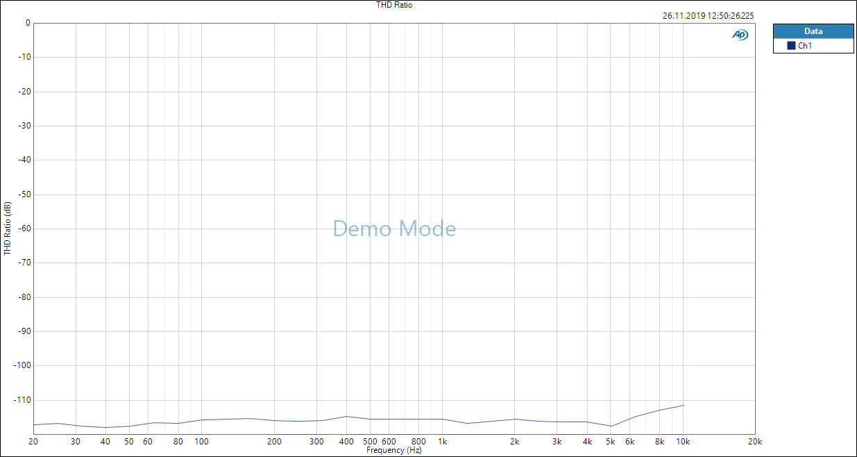
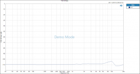
THD ratio vs frequency
Again, just THD without noise.
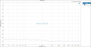
IMD: SMPTE 60 Hz + 7 kHz @ 4:1

Everything looks same like direct APx525 loopback, maybe apart from 50Hz peak coming from mains. Lab in which tests were performed is very noisy.
Frequency response
There is low pass and high pass filters at input of amp for filtering out possible DC voltage or radio frequency intererences.
APx525 is limited to only 80kHz. I also have access to Audio Precision System Two with higher bandwidth but I think such high frequencies are not meaningful anyway.
Note the scale used - 1dB max with 0.1dB step.
THD+N 1kHz vs measured power with 150Ω load
THD 1kHz vs measured power with 150Ω load
Measurement similar to previous one but only harmonic products, excluding noise
THD+N 1kHz vs measured power with 32Ω load
and for comparison
THD+N 1kHz vs level - blue channel is amplifier and red is Audio Precision loopback
THD+N ratio vs frequency
THD ratio vs frequency
Again, just THD without noise.
IMD: SMPTE 60 Hz + 7 kHz @ 4:1
Attachments
-
 SMPTE Ratio 150R.PNG37 KB · Views: 4,289
 -
 THD Ratio 150R.PNG41.3 KB · Views: 4,317
 -
 THD+N Ratio 150R.PNG40.9 KB · Views: 4,349
 -
 THD+N Ratio loopback vs 150R.png61.7 KB · Views: 4,362
 -
 THD+N Ratio vs Measured Level 32R.PNG84.6 KB · Views: 4,387
 -
 THD Ratio vs Measured Level 150R.png69.7 KB · Views: 4,429
 -
 THD+N Ratio vs Measured Level 150R.PNG69.6 KB · Views: 4,519
 -
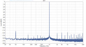 FFT 1kHz 256k 8x 2Vrms 150R.png25 KB · Views: 4,602
 -
 Relative Level (1,00000 kHz).PNG55.7 KB · Views: 4,530

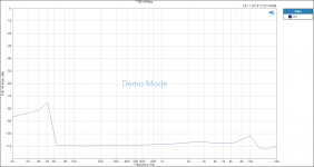
Measurements with 32 ohms load. There is some strange anomaly in THD+N vs freq graph. As I said electromagnetic environment in this bulding is very noisy and measurements were done with bare board without any shielding.
Lots of antennas are mounted on top - two radio stations, a few GSM and other devices laboratories.
THD+N vs freq looks fine on 50R so fortunately this is not problem with amplifier.
BTW. If anyone is interested I have a few spare PCBs.
Lots of antennas are mounted on top - two radio stations, a few GSM and other devices laboratories.
THD+N vs freq looks fine on 50R so fortunately this is not problem with amplifier.
BTW. If anyone is interested I have a few spare PCBs.
Attachments
Last edited:
Measurements with 32 ohms load. There is some strange anomaly in THD+N vs freq graph. As I said electromagnetic environment in this bulding is very noisy and measurements were done with bare board without any shielding.
Lots of antennas are mounted on top - two radio stations, a few GSM and other devices laboratories.
THD+N vs freq looks fine on 50R so fortunately this is not problem with amplifier.
BTW. If anyone is interested I have a few spare PCBs.
According to this, i think thd is limited by amplifier with 32r load, right?
I'm probably the last person who you would ask for describing sound. I didn't tried to compare them directly but I don't except any audible diffrences untill O2 starts to clip. My amplifier delivers consedaribly more power which may be useful with some headphones.BamboszeK,
How would you describe sound of this composite amp compared with O2?
APx525 without AG52 analog generator option is oficially specced only to -105dB THD+N. To be one hundred percent sure that distortions comes from DUT I need better analyser. I want to get Victor's oscillator and build notch filter. With this hopefully I would be able to dig deeper in distortion. Or maybe some kind member with APx555 wanna help with measurements?According to this, i think thd is limited by amplifier with 32r load, right?
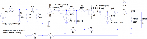
@Dave Zan suggested me some interesting stability simulation method with so called Tian Probe. Technical details could be found here and complete step by step guide for multiloop feedback analysis could be found here.
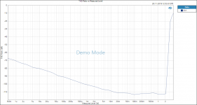
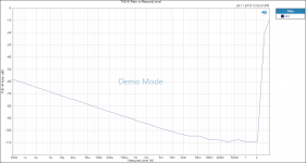
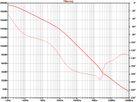
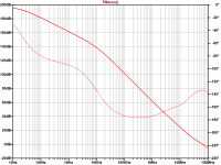
If I'm right my amplifier should have 39 dB of gain margin and 51° phase margin with 300 Ω || 10 nF load (Figure 2). With 300 Ω || 1 nF load PM is 46° and GM is infinite (Figure 3). Last graph presents Bode plot with closed loop (Figure 4).
If I'm right my amplifier should have 39 dB of gain margin and 51° phase margin with 300 Ω || 10 nF load (Figure 2). With 300 Ω || 1 nF load PM is 46° and GM is infinite (Figure 3). Last graph presents Bode plot with closed loop (Figure 4).
Attachments
I tried that already as i have such a module based on this project based on the same Burr Brown app note from 1991Hello guys,
But there is another way. PCB can be configured to take feedback post resistor/inductor. This configuration is not so popular way of isolating capacitive load from amplifier while maintaining low output impedance. I haven't tried it yet but possibility of omitting inductor is very promising.
TPA6120 Headphone Amplifier - COMPOSITE TOPOLOGY - DIY AUDIO BLOG, AUDIO WORKSHOP
https://www.ti.com/cn/lit/an/sboa002/sboa002.pdf
the pcb design for my amp was made by Vlad Palade
https://www.diyaudio.com/forums/members/palade-vlad.html
My first op-amp is OPA1642 which is fet input.
I tried many modifications on that pcb, including capacitive coupling as in the photo even modified it to look like RNHP design which has the output resistor inside the feedback loop and floating ground :
https://www.diyaudio.com/forums/hea...gh-lesson-audiophile-world-2.html#post6065578
I tried to make use of zero ohm output impedance technique in many headphones amplifiers, but it never sounded quite right...RNHP though has a non zero output impedance due to the coupling capacitors that make the floating ground . You see , Headphones aren't supposed to reproduce the base the same way as the speakers .Most expensive headphones amplifiers give less base levels and that is because of the Harman curve used by many headphones manufacturers which is tuned for more base than normal levels:
Harman tweaks its headphone target response | InnerFidelity
https://www.soundstagesolo.com/index.php/features/217-where-are-we-at-with-the-harman-curve
Attachments
Last edited:
Agree, making NFB past resistor resolve high current/ high output impedance issue. But what about your research with inductor at the output, you can't leave IC unprotected against over current/ over temperature - no-go to end product. Is it just theoretical work on the two decades old and quite expensive amplifier w/o practical meaning?use it as Neve's RNHP does and you don't need any protection...
Actually TPA6120A2 is short-circuit and thermally protected.TPA6120 is interesting for output buffering, but I can't see if it has any short circuits protection. TI recommends 40 Ohm series resistor as anti-oscillation, though may be dual-role for this resistor - current limiting as well.
That was my concern also. TRS Jack used widely in headphones is known for its shorting capability.
THS6012 is same chip as TPA6120A2 and as datasheet states "Thermal Shutdown and Short Circuit Protection".
https://www.ti.com/lit/ds/symlink/ths6012.pdf
TI guys confirms that same is true for TPA6120A2 - https://e2e.ti.com/support/audio/f/6/t/377352?TPA6120A2-Short-Circuit-protection
However, such high current (800mA) and power capability might be dangerous for some headphones.
For stability 10 ohms are sufficient.
I'm aiming for zero output impedance so additional inductor was used. Sticking to high output impedance would make it lot easier to stabilize.
There is old IEC standard for 120 ohms output impedance for headphone amplifiers, but AFAIK the vast majority of currently produced headphones are designed for maximum electrical damping factor.
I'm using Sonarworks for headphone frequency response correction which IMHO yelds great results. I need to also try this free software. GitHub - jaakkopasanen/AutoEq: Automatic headphone equalization from frequency responses They use Harman target with their measurements.
Last edited:
There is a note (2) and (3) on page 4 of the tpa6120 data sheet:Actually TPA6120A2 is short-circuit and thermally protected.
That was my concern also. TRS Jack used widely in headphones is known for its shorting capability.
THS6012 is same chip as TPA6120A2 and as datasheet states "Thermal Shutdown and Short Circuit Protection".
https://www.ti.com/lit/ds/symlink/ths6012.pdf
TI guys confirms that same is true for TPA6120A2 - https://e2e.ti.com/support/audio/f/6/t/377352?TPA6120A2-Short-Circuit-protection
It tells me that no input, no output protection. And 700 mA output "typical" current value imply 20 Ohm Rds MOSFET limit, that may go up to anything - TI didn't specify "max".When the TPA6120A2 is powered down, the input source voltage must be kept below 600mV peak.
The TPA6120A2 incorporates an exposed PowerPAD on the underside of the chip. This acts as a heatsink and must be connected to a
thermally dissipating plane for proper power dissipation. Failure to do so may result in exceeding the maximum junction temperature that
could permanently damage the device. See TI Technical Brief SLMA002 for more information about utilizing the PowerPAD thermally
enhanced package.
Actually i was talking about the split capacitance that forms the virtual ground , which is naturally protecting the headphones from dc current surge.I am not using the output resistor inside the feedback network.On my headphones it sounds better with a series resistor thus with lower DF. The IC is like 3 $ each, my headphones are 200 $ now...Agree, making NFB past resistor resolve high current/ high output impedance issue. But what about your research with inductor at the output, you can't leave IC unprotected against over current/ over temperature - no-go to end product. Is it just theoretical work on the two decades old and quite expensive amplifier w/o practical meaning?
There is a note (2) and (3) on page 4 of the tpa6120 data sheet:
It tells me that no input, no output protection. And 700 mA output "typical" current value imply 20 Ohm Rds MOSFET limit, that may go up to anything - TI didn't specify "max".
I really don't know where you see problem. Previous stage, the OPA1602 is fully input protected. They are powered at same time. There is no way to inject any signal to TPA6120A2 when it is powered down becouse OPA1602 would be powered down also.
TPA6120A2 is made in bipolar process. I don't see any MOSFETs here.
TI simply stated that it is required, not optional to connect power tab to groundplane. Without any groundplane acting as heatsink, device will heat up quickly. Even with only only quiescent currents.
IMHO TPA6120A2 is perfectly fine and safe for driving headphones. User should watch out for potenitiometer position but it is true for any high powered amp. I consider adding relay and microcontroller based extensive protection but mostly as programming exercise rather than serious need.
AD8397 is much more dangerous as it doesn't incorporate any kind of protection. I've personaly seen and fixed faulty headphone amplifier using this IC which had 15V DC at output. It destroyed expensive headphones by simply plugging headphone jack. And this amplifier had series resistance at output.
Actually TPA6120A2 is short-circuit and thermally protected...........
THS6012... "Continuous output shorts are not recommended and could damage the device."
- Home
- Amplifiers
- Headphone Systems
- High performance OPA1602 + TPA6120A2 Composite Headphone Amplifier