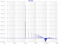
The graph is unusual too (I have never simulated anything that has zero features before)
Not to burst your bubble too much, but THD is one of those things that is often not covered well in the simulation models. Your sim shows that you didn't make any obvious mistakes. I highly doubt measurements of the circuit will come even remotely close to the simulated values.
Regardless, it should still be a pretty nice amp. Watch the power dissipation in those itty-bitty packages, though.
Tom
Here is an interesting surprise, I replaced the LME47720, the supposedly "king of the low THD" opamps in TI's arsenal, with the lowly OPA1688 (which is also serving as the buffer).
Simulations of THD, while using only basic functional opamp models, make no sense. It will not produce any meaningful result. Those models are made from a bunch of controlled voltage and current sources. The only nonlinear effect they usually take into account is supply rail clipping.
There are transistor level models of opamps, but the one you have is not one of them.
For comparison, somewhat similar nested feedback circuit perfomance:
OPA1611 "The Crocodile"
vs
OPA172 - "The Crocodile"
LME49720 is a bit more nonlinear in those conditions compare to OPA1661, but not by a huge lot.
Last edited:
You can open a model in a text editor and have a look what it contains.
Some models have an input stage "made of" transistors, to model noises and other effects associated with an input, and the rest of it made with controlled sources.
The fact that it runs a low does not say a lot. It may be happening because something makes spice to use very small timestep and not because if complexity of a model.
Those models are made from a bunch of controlled voltage and current sources. The only nonlinear effect they usually take into account is supply rail clipping.
Here is the OPA1688 model from TI. The following are modeled (see bold below) - seems quite comprehensive to me
* OPEN-LOOP GAIN AND PHASE VS. FREQUENCY WITH RL, CL EFFECTS (Aol)
* UNITY GAIN BANDWIDTH (GBW)
* INPUT COMMON-MODE REJECTION RATIO VS. FREQUENCY (CMRR)
* POWER SUPPLY REJECTION RATIO VS. FREQUENCY (PSRR)
* DIFFERENTIAL INPUT IMPEDANCE (Zid)
* COMMON-MODE INPUT IMPEDANCE (Zic)
* OPEN-LOOP OUTPUT IMPEDANCE VS. FREQUENCY (Zo)
* OUTPUT CURRENT THROUGH THE SUPPLY (Iout)
* INPUT VOLTAGE NOISE DENSITY VS. FREQUENCY (en)
* INPUT CURRENT NOISE DENSITY VS. FREQUENCY (in)
* OUTPUT VOLTAGE SWING vs. OUTPUT CURRENT (Vo)
* SHORT-CIRCUIT OUTPUT CURRENT (Isc)
* QUIESCENT CURRENT (Iq)
* SETTLING TIME VS. CAPACITIVE LOAD (ts)
* SLEW RATE (SR)
* SMALL SIGNAL OVERSHOOT VS. CAPACITIVE LOAD
* LARGE SIGNAL RESPONSE
* OVERLOAD RECOVERY TIME (tor)
* INPUT BIAS CURRENT (Ib)
* INPUT OFFSET CURRENT (Ios)
* INPUT OFFSET VOLTAGE (Vos)
* INPUT COMMON-MODE VOLTAGE RANGE (Vcm)
* INPUT OFFSET VOLTAGE VS. INPUT COMMON-MODE VOLTAGE (Vos vs. Vcm)
* INPUT/OUTPUT ESD CELLS (ESDin, ESDout)
Code:
*$
* OPA1688
*****************************************************************************
* (C) Copyright 2018 Texas Instruments Incorporated. All rights reserved.
*****************************************************************************
** This model is designed as an aid for customers of Texas Instruments.
** TI and its licensors and suppliers make no warranties, either expressed
** or implied, with respect to this model, including the warranties of
** merchantability or fitness for a particular purpose.  The model is
** provided solely on an "as is" basis.  The entire risk as to its quality
** and performance is with the customer
*****************************************************************************
*
* This model is subject to change without notice. Texas Instruments
* Incorporated is not responsible for updating this model.
*
*****************************************************************************
*
** Released by: Online Design Tools, Texas Instruments Inc.
* Part: OPA1688
* Date: 03JUL2018
* Model Type: Generic (suitable for all analysis types)
* EVM Order Number: N/A
* EVM Users Guide:  N/A
* Datasheet: SBOS724 –SEPTEMBER 2015
* Created with Green-Williams-Lis Op Amp Macro-model Architecture
*
* Model Version: Final 1.0
*
*****************************************************************************
*
* Final 1.0
* Release to Web.
*
*****************************************************************************
* Model Usage Notes:
* 1. The following parameters are modeled:
* 		OPEN-LOOP GAIN AND PHASE VS. FREQUENCY  WITH RL, CL EFFECTS (Aol)
* 		UNITY GAIN BANDWIDTH (GBW)
* 		INPUT COMMON-MODE REJECTION RATIO VS. FREQUENCY (CMRR)
* 		POWER SUPPLY REJECTION RATIO VS. FREQUENCY (PSRR)
* 		DIFFERENTIAL INPUT IMPEDANCE (Zid)
* 		COMMON-MODE INPUT IMPEDANCE (Zic)
* 		OPEN-LOOP OUTPUT IMPEDANCE VS. FREQUENCY (Zo)
* 		OUTPUT CURRENT THROUGH THE SUPPLY (Iout)
* 		INPUT VOLTAGE NOISE DENSITY VS. FREQUENCY (en)
* 		INPUT CURRENT NOISE DENSITY VS. FREQUENCY (in)
* 		OUTPUT VOLTAGE SWING vs. OUTPUT CURRENT (Vo)
* 		SHORT-CIRCUIT OUTPUT CURRENT (Isc)
* 		QUIESCENT CURRENT (Iq)
* 		SETTLING TIME VS. CAPACITIVE LOAD (ts)
* 		SLEW RATE (SR)
* 		SMALL SIGNAL OVERSHOOT VS. CAPACITIVE LOAD
* 		LARGE SIGNAL RESPONSE
* 		OVERLOAD RECOVERY TIME (tor)
* 		INPUT BIAS CURRENT (Ib)
* 		INPUT OFFSET CURRENT (Ios)
* 		INPUT OFFSET VOLTAGE (Vos)
* 		INPUT COMMON-MODE VOLTAGE RANGE (Vcm)
* 		INPUT OFFSET VOLTAGE VS. INPUT COMMON-MODE VOLTAGE (Vos vs. Vcm)
* 		INPUT/OUTPUT ESD CELLS (ESDin, ESDout)
* 2. Model represent the device operating at room temperature only. No temperature dependency is modeled
******************************************************
.subckt OPA1688 IN+ IN- VCC VEE OUT
******************************************************
.model BB_SW VSWITCH(Ron=50 Roff=1e12 Von=700e-3 Voff=0)
.model ESD_SW VSWITCH(Ron=50 Roff=1e12 Von=250e-3 Voff=0)
.model OL_SW VSWITCH(Ron=1e-3 Roff=1e9 Von=900e-3 Voff=800e-3)
.model OR_SW VSWITCH(Ron=10e-3 Roff=1e9 Von=10e-3 Voff=0)
.model R_NOISELESS RES(T_ABS=-273.15)
******************************************************
V_ORn       33 VCLP -1.642
V_ORp       34 VCLP 1.65
V_OS        39 40 214.2U
V4          ZO_OUT_J1 OUT 0
V_GRp       53 MID 175
V_GRn       54 MID -175
V_ISCp      49 MID 74.98
V_ISCn      50 MID -75.98
V11         44 48 0
V12         43 47 0
VCM_MIN     67 VEE_B -100M
VCM_MAX     68 VCC_B -2
I_Q         VCC VEE 1.6M
I_OS        ESDn MID 7P
I_B         40 MID 10P
XU3         OUT_21 VEE_B MID PSRR_CMRR_0
XIn11       ESDn MID FEMT_0
XCLAW_SRC   22 23 CLAW_CLAMP MID VCCS_LIM_3_0
XU1 Zo_Cleft CL_CLAMP Zo_Cright MID ZO_OUT_J1 AOL_INN_J1 AOL_INP_J1 CLAMP
+ CLAW_CLAMP VSENSE AOL_ZO_0
XU5         VEE VCC ESDn ESDp ESD_0
C_DIFF      ESDp ESDn 7P
S7          VEE OUT VEE OUT  S_VSWITCH_1
S6          OUT VCC OUT VCC  S_VSWITCH_2
XU4         OUT_J1_29 ESDp MID PSRR_CMRR_1
XU2         OUT_J1_30 VCC_B MID PSRR_CMRR_2
XGR_SRC     31 32 CLAMP MID VCCS_LIM_GR_0
XCL_SRC     35 36 CL_CLAMP MID VCCS_LIM_4_0
XCLAWp      VIMON MID 37 VCC_B VCCS_LIM_CLAW+_0
XCLAWn      MID VIMON VEE_B 38 VCCS_LIM_CLAW-_0
Xe_n        40 ESDp VNSE_0
Xi_np       MID 40 FEMT_0
H2          41 MID V11 -1
H3          42 MID V12 1
S1          Zo_Cleft Zo_Cright SW_OL MID  S_VSWITCH_3
SOR_SWp     CLAMP 43 CLAMP 43  S_VSWITCH_4
SOR_SWn     44 CLAMP 44 CLAMP  S_VSWITCH_5
C_CMn       ESDn MID 1.5P
C_CMp       MID ESDp 1.5P
C28         45 MID 1P
R77         42 45 R_NOISELESS 100
C27         46 MID 1P
R76         41 46 R_NOISELESS 100
R75         MID 47 R_NOISELESS 1
GVCCS8      47 MID 34 MID  -1
R74         48 MID R_NOISELESS 1
GVCCS7      48 MID 33 MID  -1
XIQPos      VIMON MID MID VCC VCCS_LIMIT_IQ_0
XIQNeg      MID VIMON VEE MID VCCS_LIMIT_IQ_0
XCL_AMP     49 50 VIMON MID 51 52 CLAMP_AMP_LO_0_0
XGR_AMP     53 54 55 MID 56 57 CLAMP_AMP_HI_0
R39         53 MID R_NOISELESS 1T
R37         54 MID R_NOISELESS 1T
R42         VSENSE 55 R_NOISELESS 1M
C19         55 MID 1F
R38         56 MID R_NOISELESS 1
R36         MID 57 R_NOISELESS 1
R40         56 31 R_NOISELESS 1M
R41         57 32 R_NOISELESS 1M
C17         31 MID 1F
C18         MID 32 1F
R21         51 MID R_NOISELESS 1
R20         MID 52 R_NOISELESS 1
R29         51 35 R_NOISELESS 1M
R30         52 36 R_NOISELESS 1M
C9          35 MID 1F
C8          MID 36 1F
R22         49 MID R_NOISELESS 1T
R19         MID 50 R_NOISELESS 1T
R12         37 VCC_B R_NOISELESS 1K
R16         37 58 R_NOISELESS 1M
R13         VEE_B 38 R_NOISELESS 1K
R17         59 38 R_NOISELESS 1M
C6          59 MID 0.1p
C5          MID 58 0.1p
G2          VCC_CLP MID 58 MID  -1M
R15         VCC_CLP MID R_NOISELESS 1K
G3          VEE_CLP MID 59 MID  -1M
R14         MID VEE_CLP R_NOISELESS 1K
XCLAW_AMP   VCC_CLP VEE_CLP VOUT_S MID 60 61 CLAMP_AMP_LO_0
R26         VCC_CLP MID R_NOISELESS 1T
R23         VEE_CLP MID R_NOISELESS 1T
R25         60 MID R_NOISELESS 1
R24         MID 61 R_NOISELESS 1
R27         60 22 R_NOISELESS 1M
R28         61 23 R_NOISELESS 1M
C11         22 MID 1F
C10         MID 23 1F
C12         SW_OL MID 100P
R32         62 SW_OL R_NOISELESS 100
R31         62 MID R_NOISELESS 1
XOL_SENSE   MID 62 46 45 OL_SENSE_0
H1          63 MID V4 1K
R11         MID 64 R_NOISELESS 1T
R18         64 VOUT_S R_NOISELESS 100
C7          VOUT_S MID 1N
E2          64 MID OUT MID  1
C13         VIMON MID 1N
R33         63 VIMON R_NOISELESS 100
R10         MID 63 R_NOISELESS 1T
R47         65 VCLP R_NOISELESS 100
C24         VCLP MID 100P
E4          65 MID CL_CLAMP MID  1
C4          AOL_INP_J1 MID 1F
R9          AOL_INP_J1 66 R_NOISELESS 1M
R7          MID 67 R_NOISELESS 1T
R6          68 MID R_NOISELESS 1T
R8          MID 66 R_NOISELESS 1
XVCM_CLAMP  69 MID 66 MID 68 67 VCCS_EXT_LIM_0
E1          MID 0 70 0  1
R89         VEE_B 0 R_NOISELESS 1
R5          71 VEE_B R_NOISELESS 1M
C3          71 0 1F
R60         70 71 R_NOISELESS 1MEG
C1          70 0 1
R3          70 0 R_NOISELESS 1T
R59         72 70 R_NOISELESS 1MEG
C2          72 0 1F
R4          VCC_B 72 R_NOISELESS 1M
R88         VCC_B 0 R_NOISELESS 1
G17         VEE_B 0 VEE 0  -1
G16         VCC_B 0 VCC 0  -1
R_PSR       73 69 R_NOISELESS 1K
G1          69 73 OUT_J1_30 OUT_21  -1M
R2          AOL_INN_J1 ESDn R_NOISELESS 1M
R1          73 74 R_NOISELESS 1M
R_CMR       39 74 R_NOISELESS 1K
G5          74 39 OUT_J1_29 MID  -1M
R53         ESDn MID R_NOISELESS 1T
R52         MID ESDp R_NOISELESS 1T
R35         IN- ESDn R_NOISELESS 250
R34         IN+ ESDp R_NOISELESS 250
.MODEL S_VSWITCH_1 VSWITCH (RON=50 ROFF=1T VON=500M VOFF=450M)
.MODEL S_VSWITCH_2 VSWITCH (RON=50 ROFF=1T VON=500M VOFF=450M)
.MODEL S_VSWITCH_3 VSWITCH (RON=1M ROFF=1G VON=900M VOFF=800M)
.MODEL S_VSWITCH_4 VSWITCH (RON=10M ROFF=1G VON=10M VOFF=0)
.MODEL S_VSWITCH_5 VSWITCH (RON=10M ROFF=1G VON=10M VOFF=0)
.ENDS OPA1688
*
.SUBCKT PSRR_CMRR_0 psrr_in psrr_vccb psrr_mid
R80         psrr_mid psrr_in R_RES_1 10.6250124K
C27         psrr_in 4_75 166.45P
R79         4_75 psrr_in R_RES_2 100MEG
GVCCS8      4_75 psrr_mid psrr_vccb psrr_mid  -9.4128M
R78         psrr_mid 4_75 R_RES_3 1
.MODEL R_RES_1 RES ( TCE=0 T_ABS=-273.15)
.MODEL R_RES_2 RES ( TCE=0 T_ABS=-273.15)
.MODEL R_RES_3 RES ( TCE=0 T_ABS=-273.15)
.ENDS
*
.SUBCKT AOL_ZO_0 ZO_CLEFT CL_CLAMP ZO_CRIGHT MID ZO_OUT AOL_INN AOL_INP CLAMP
+ CLAW_CLAMP VSENSE
R4_VS       MID VSENSE R_RES_1 1K
GVCCS4_VS   VSENSE MID CLAMP MID  -1M
GVCCS4      79 MID 78 MID  -1
C5          80 MID 16.422P
R11         78 80 R_RES_2 10K
R10         78 81 R_RES_3 3.2175909091MEG
R9          81 MID R_RES_4 1
GVCCS1      81 MID 82 MID  -276.2764
C1          83 82 2.0527U
R3          82 MID R_RES_5 36.3271
R2          82 83 R_RES_6 10K
R1          83 MID R_RES_7 1
R1_2        84 MID 1
XVCCS_LIM_ZO 85 MID MID 84 VCCS_LIM_ZO_0
R11_2       85 MID R_RES_8 1.2502
C4_2        85 79 636.62F
R10_2       85 79 R_RES_9 10K
R9_2        79 MID R_RES_10 1
GVCCS1_1    83 MID ZO_CRIGHT MID  -1.4474
C1_1        ZO_CLEFT ZO_CRIGHT 5.5583U
R2_1        ZO_CRIGHT MID R_RES_11 22.3514424K
R1_1        ZO_CRIGHT ZO_CLEFT R_RES_12 10K
Rdummy      MID ZO_OUT R_RES_13 1K
Rx          ZO_OUT 84 R_RES_14 10K
Rdc_1       ZO_CLEFT MID R_RES_15 1
G_Aol_Zo    ZO_CLEFT MID CL_CLAMP ZO_OUT  -89.0549
C3          86 87 144.7F
R12         87 MID R_RES_16 111.2
R8          87 86 R_RES_17 10K
R7          86 MID R_RES_18 1
GVCCS3      86 MID 88 MID  -90.91
C2          89 88 159.2F
R6          88 MID R_RES_19 101
R5          88 89 R_RES_20 10K
R4          89 MID R_RES_21 1
GVCCS2      89 MID out2 MID  -100
C2_A2       out2 MID 8F
R3_A2       MID out2 R_RES_22 1MEG
GVCCS3_A2   out2 MID VSENSE MID  -1U
XVCCS_LIM_2 4_A0 MID MID CLAMP VCCS_LIM_2_0
C1_A0       CLAMP MID 40.5N
R4_A0       MID CLAMP R_RES_23 1MEG
R3_A0       MID 4_A0 R_RES_24 1MEG
XVCCS_LIM_1 AOL_INP AOL_INN MID 4_A0 VCCS_LIM_1_0
R4_CL       MID CL_CLAMP R_RES_25 1K
GVCCS4_CL   CL_CLAMP MID CLAW_CLAMP MID  -1M
R4_CC       MID CLAW_CLAMP R_RES_26 1K
GVCCS4_CC   CLAW_CLAMP MID 87 MID  -1M
.MODEL R_RES_1 RES ( TCE=0 T_ABS=-273.15)
.MODEL R_RES_2 RES ( TCE=0 T_ABS=-273.15)
.MODEL R_RES_3 RES ( TCE=0 T_ABS=-273.15)
.MODEL R_RES_4 RES ( TCE=0 T_ABS=-273.15)
.MODEL R_RES_5 RES ( TCE=0 T_ABS=-273.15)
.MODEL R_RES_6 RES ( TCE=0 T_ABS=-273.15)
.MODEL R_RES_7 RES ( TCE=0 T_ABS=-273.15)
.MODEL R_RES_8 RES ( TCE=0 T_ABS=-273.15)
.MODEL R_RES_9 RES ( TCE=0 T_ABS=-273.15)
.MODEL R_RES_10 RES ( TCE=0 T_ABS=-273.15)
.MODEL R_RES_11 RES ( TCE=0 T_ABS=-273.15)
.MODEL R_RES_12 RES ( TCE=0 T_ABS=-273.15)
.MODEL R_RES_13 RES ( TCE=0 T_ABS=-273.15)
.MODEL R_RES_14 RES ( TCE=0 T_ABS=-273.15)
.MODEL R_RES_15 RES ( TCE=0 T_ABS=-273.15)
.MODEL R_RES_16 RES ( TCE=0 T_ABS=-273.15)
.MODEL R_RES_17 RES ( TCE=0 T_ABS=-273.15)
.MODEL R_RES_18 RES ( TCE=0 T_ABS=-273.15)
.MODEL R_RES_19 RES ( TCE=0 T_ABS=-273.15)
.MODEL R_RES_20 RES ( TCE=0 T_ABS=-273.15)
.MODEL R_RES_21 RES ( TCE=0 T_ABS=-273.15)
.MODEL R_RES_22 RES ( TCE=0 T_ABS=-273.15)
.MODEL R_RES_23 RES ( TCE=0 T_ABS=-273.15)
.MODEL R_RES_24 RES ( TCE=0 T_ABS=-273.15)
.MODEL R_RES_25 RES ( TCE=0 T_ABS=-273.15)
.MODEL R_RES_26 RES ( TCE=0 T_ABS=-273.15)
.ENDS
*
.SUBCKT ESD_0 VEE VCC ESDn ESDp
SW5         ESDp ESDn ESDp ESDn  S_VSWITCH_1
SW6         ESDn ESDp ESDn ESDp  S_VSWITCH_2
SW1         VEE ESDp VEE ESDp  S_VSWITCH_3
SW3         VEE ESDn VEE ESDn  S_VSWITCH_4
SW4         ESDn VCC ESDn VCC  S_VSWITCH_5
SW2         ESDp VCC ESDp VCC  S_VSWITCH_6
.MODEL S_VSWITCH_1 VSWITCH (RON=50 ROFF=1T VON=700M VOFF=650M)
.MODEL S_VSWITCH_2 VSWITCH (RON=50 ROFF=1T VON=700M VOFF=650M)
.MODEL S_VSWITCH_3 VSWITCH (RON=50 ROFF=1T VON=500M VOFF=450M)
.MODEL S_VSWITCH_4 VSWITCH (RON=50 ROFF=1T VON=500M VOFF=450M)
.MODEL S_VSWITCH_5 VSWITCH (RON=50 ROFF=1T VON=500M VOFF=450M)
.MODEL S_VSWITCH_6 VSWITCH (RON=50 ROFF=1T VON=500M VOFF=450M)
.ENDS
*
.SUBCKT PSRR_CMRR_1 OUT IN MID
G_2         OUT MID 90 MID  -250
R74         MID OUT R_RES_1 1
R2a         MID 91 R_RES_2 100.1001001K
C1a         91 92 79.577F
R48         92 91 R_RES_3 100MEG
G_1         92 MID IN MID  -1M
Rsrc        MID 92 R_RES_4 1
R2b         MID 90 R_RES_5 401.6064257K
C2a         90 93 39.789F
R73         93 90 R_RES_6 100MEG
GVCCS1      93 MID 91 MID  -1
R49         MID 93 R_RES_7 1
.MODEL R_RES_1 RES ( TCE=0 T_ABS=-273.15)
.MODEL R_RES_2 RES ( TCE=0 T_ABS=-273.15)
.MODEL R_RES_3 RES ( TCE=0 T_ABS=-273.15)
.MODEL R_RES_4 RES ( TCE=0 T_ABS=-273.15)
.MODEL R_RES_5 RES ( TCE=0 T_ABS=-273.15)
.MODEL R_RES_6 RES ( TCE=0 T_ABS=-273.15)
.MODEL R_RES_7 RES ( TCE=0 T_ABS=-273.15)
.ENDS
*
.SUBCKT PSRR_CMRR_2 OUT IN MID
R80         MID OUT R_RES_1 2.5000625K
C27         OUT 4_94 3.1831P
R79         4_94 OUT R_RES_2 100MEG
GVCCS8      4_94 MID IN MID  -40M
R78         MID 4_94 R_RES_3 1
.MODEL R_RES_1 RES ( TCE=0 T_ABS=-273.15)
.MODEL R_RES_2 RES ( TCE=0 T_ABS=-273.15)
.MODEL R_RES_3 RES ( TCE=0 T_ABS=-273.15)
.ENDS
*
.SUBCKT FEMT_0  1 2
.PARAM FLWF=0.001
.PARAM NLFF=1.8
.PARAM NVRF=1.8
.PARAM GLFF={PWR(FLWF,0.25)*NLFF/1164}
.PARAM RNVF={1.184*PWR(NVRF,2)}
.MODEL DVNF D KF={PWR(FLWF,0.5)/1E11} IS=1.0E-16
I1 0 7 10E-3
I2 0 8 10E-3
D1 7 0 DVNF
D2 8 0 DVNF
E1 3 6 7 8 {GLFF}
R1 3 0 1E9
R2 3 0 1E9
R3 3 6 1E9
E2 6 4 5 0 10
R4 5 0 {RNVF}
R5 5 0 {RNVF}
R6 3 4 1E9
R7 4 0 1E9
G1 1 2 3 4 1E-6
.ENDS
*
.SUBCKT VCCS_LIM_3_0  VC+ VC- IOUT+ IOUT-
.PARAM GAIN = 1
.PARAM IPOS = 10
.PARAM INEG = -10
G1 IOUT+ IOUT- VALUE={LIMIT(GAIN*V(VC+,VC-),INEG,IPOS)}
.ENDS
*
.SUBCKT VCCS_LIM_GR_0  VC+ VC- IOUT+ IOUT-
.PARAM GAIN = 1
.PARAM IPOS = 100
.PARAM INEG = -100
G1 IOUT+ IOUT- VALUE={LIMIT(GAIN*V(VC+,VC-),INEG,IPOS)}
.ENDS
*
.SUBCKT VCCS_LIM_4_0  VC+ VC- IOUT+ IOUT-
.PARAM GAIN = 1
.PARAM IPOS = 20
.PARAM INEG = -20
G1 IOUT+ IOUT- VALUE={LIMIT(GAIN*V(VC+,VC-),INEG,IPOS)}
.ENDS
*
.SUBCKT VCCS_LIM_CLAW+_0  VC+ VC- IOUT+ IOUT-
G1 IOUT+ IOUT- TABLE {ABS(V(VC+,VC-))} =
+(3.55E-15, 0)
+(10.0409, 0.0003165)
+(19.5806, 0.0006332)
+(39.9131, 0.0012661)
+(49.9586, 0.0016743)
+(60.011, 0.0022202)
+(66.47, 2.7E-3)
+(68.8242, 0.0030418)
+(72.6386, 0.004141)
+(74.9241, 0.0047363)
.ENDS
*
.SUBCKT VCCS_LIM_CLAW-_0  VC+ VC- IOUT+ IOUT-
G1 IOUT+ IOUT- TABLE {ABS(V(VC+,VC-))} =
+(0, 1.71E-05)
+(23.5589, 4.71E-05)
+(30.0752, 0.0003883)
+(40.1003, 0.0008738)
+(50.1253, 0.0014563)
+(59.6491, 0.0020874)
+(66.9173, 0.0026699)
+(70.1754, 0.0030583)
+(74.6867, 0.0040291)
+(75.9798, 0.0044175)
.ENDS
*
.SUBCKT VNSE_0  1 2
.PARAM FLW=0.1
.PARAM NLF=380
.PARAM NVR=6
.PARAM GLF={PWR(FLW,0.25)*NLF/1164}
.PARAM RNV={1.184*PWR(NVR,2)}
.MODEL DVN D KF={PWR(FLW,0.5)/1E11} IS=1.0E-16
I1 0 7 10E-3
I2 0 8 10E-3
D1 7 0 DVN
D2 8 0 DVN
E1 3 6 7 8 {GLF}
R1 3 0 1E9
R2 3 0 1E9
R3 3 6 1E9
E2 6 4 5 0 10
R4 5 0 {RNV}
R5 5 0 {RNV}
R6 3 4 1E9
R7 4 0 1E9
E3 1 2 3 4 1
.ENDS
*
.SUBCKT VCCS_LIMIT_IQ_0  VC+ VC- IOUT+ IOUT-
.PARAM GAIN = 1E-3
G1 IOUT- IOUT+ VALUE={IF( (V(VC+,VC-)<=0),0,GAIN*V(VC+,VC-) )}
.ENDS
*
.SUBCKT CLAMP_AMP_LO_0_0   VC+ VC- VIN COM VO+ VO-
.PARAM G=1
GVO+ COM VO+ VALUE = {IF(V(VIN,COM)>V(VC+,COM),((V(VIN,COM)-V(VC+,COM))*G),0)}
GVO- COM VO- VALUE = {IF(V(VIN,COM)<V(VC-,COM),((V(VC-,COM)-V(VIN,COM))*G),0)}
.ENDS
*
.SUBCKT CLAMP_AMP_HI_0  VC+ VC- VIN COM VO+ VO-
.PARAM G=10
GVO+ COM VO+ VALUE = {IF(V(VIN,COM)>V(VC+,COM),((V(VIN,COM)-V(VC+,COM))*G),0)}
GVO- COM VO- VALUE = {IF(V(VIN,COM)<V(VC-,COM),((V(VC-,COM)-V(VIN,COM))*G),0)}
.ENDS
*
.SUBCKT CLAMP_AMP_LO_0  VC+ VC- VIN COM VO+ VO-
.PARAM G=1
GVO+ COM VO+ VALUE = {IF(V(VIN,COM)>V(VC+,COM),((V(VIN,COM)-V(VC+,COM))*G),0)}
GVO- COM VO- VALUE = {IF(V(VIN,COM)<V(VC-,COM),((V(VC-,COM)-V(VIN,COM))*G),0)}
.ENDS
*
.SUBCKT OL_SENSE_0  COM SW+ OLN  OLP
GSW+ COM SW+ VALUE = {IF((V(OLN,COM)>10E-3 | V(OLP,COM)>10E-3),1,0)}
.ENDS
*
.SUBCKT VCCS_EXT_LIM_0  VIN+ VIN- IOUT- IOUT+ VP+ VP-
.PARAM GAIN = 1
G1 IOUT+ IOUT- VALUE={LIMIT(GAIN*V(VIN+,VIN-),V(VP-,VIN-), V(VP+,VIN-))}
.ENDS
*
.SUBCKT VCCS_LIM_ZO_0  VC+ VC- IOUT+ IOUT-
.PARAM GAIN = 8000
.PARAM IPOS = 1300e3
.PARAM INEG = -1407.599e3
G1 IOUT+ IOUT- VALUE={LIMIT(GAIN*V(VC+,VC-),INEG,IPOS)}
.ENDS
*
.SUBCKT VCCS_LIM_2_0  VC+ VC- IOUT+ IOUT-
.PARAM GAIN = 0.03675
.PARAM IPOS = 0.35
.PARAM INEG = -0.35
G1 IOUT+ IOUT- VALUE={LIMIT(GAIN*V(VC+,VC-),INEG,IPOS)}
.ENDS
*
.SUBCKT VCCS_LIM_1_0  VC+ VC- IOUT+ IOUT-
.PARAM GAIN = 1E-4
.PARAM IPOS = .5
.PARAM INEG = -.5
G1 IOUT+ IOUT- VALUE={LIMIT(GAIN*V(VC+,VC-),INEG,IPOS)}
.ENDS
*
Last edited:
As i was saying, it does not contain a single transistor. Modeling distortion with this model useless.
There was no even need to go that far, it was obvious from spectrum you posted.
BTW, whatever it says this model covers in its headline is often far from being real. Yes, those header can lie")
There was no even need to go that far, it was obvious from spectrum you posted.
BTW, whatever it says this model covers in its headline is often far from being real. Yes, those header can lie
It appears to be a phenomenological model not a network of discrete actives. That doesn’t automatically make something “useless” - a company like TI with armies of engineers would probably not release useless models of their parts.
With Lser=0.15ohms for the PSU rails, the distortion sims are higher in THD and probably closer to reality. it really is sensitive to the series resistance of the power supply rails. The cases before were idealized ultralow ESR cases.
Here is 28Vpp into 50ohms with PSU Lser=0.15ohms:
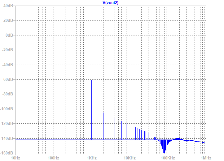
FFT Components:
So it does respond to changes in circuit design and is not stuck at zero THD. Also note that the character of the HD is descending higher orders with dominant 2nd order, whereas the LME49720 has dominant 3rd order as shown in Post 1.
With Lser=0.15ohms for the PSU rails, the distortion sims are higher in THD and probably closer to reality. it really is sensitive to the series resistance of the power supply rails. The cases before were idealized ultralow ESR cases.
Here is 28Vpp into 50ohms with PSU Lser=0.15ohms:
FFT Components:
Harmonic Frequency Fourier Normalized Phase Normalized
Number [Hz] Component Component [degree] Phase [deg]
1 1.000e+03 1.402e+01 1.000e+00 -0.04° 0.00°
2 2.000e+03 7.864e-06 5.609e-07 -178.42° -178.37°
3 3.000e+03 8.375e-09 5.974e-10 -5.85° -5.80°
4 4.000e+03 3.135e-06 2.236e-07 -176.02° -175.97°
5 5.000e+03 1.392e-08 9.926e-10 -3.43° -3.39°
6 6.000e+03 2.004e-06 1.430e-07 -173.77° -173.73°
7 7.000e+03 1.946e-08 1.388e-09 -2.37° -2.32°
8 8.000e+03 1.473e-06 1.051e-07 -171.53° -171.49°
9 9.000e+03 2.501e-08 1.784e-09 -1.75° -1.70°
Total Harmonic Distortion: 0.000063%(0.000000%)
So it does respond to changes in circuit design and is not stuck at zero THD. Also note that the character of the HD is descending higher orders with dominant 2nd order, whereas the LME49720 has dominant 3rd order as shown in Post 1.
Attachments
Last edited:
It appears to be a phenomenological model not a network of discrete actives. That doesn’t automatically make something “useless” - a company like TI with armies of engineers would probably not release useless models of their parts.
First off, TI does not have "armies of engineers". When I worked there, we were all stretched pretty thin. Secondly, just because something is not "useless" does not mean that it is useful.
Models will always have their limitations. When you model something, you usually get to choose between having a model that fits broadly but isn't super precise, or a model that is very precise within a narrow operating range.
I think TI did pretty well in their modelling of the OPA1688 - at least judging by the feature list. All the important stuff is there: Small signal response, large signal response, loop gain/phase, etc. But you will also notice that THD is not on the list.
Your notion that "it takes a long time to simulate, therefore it must be a really good model" is laughable. The reason it takes a long time to simulate is most likely that the simulator has a hard time getting the simulation to converge on a DC solution so it can start the transient sim.
You've already shown the world that you have an amp that's probably not broken. Now do yourself a favour: Build it and measure it. Have a listen.
Tom
Tomchr,
Let’s not put words in my mouth.
You “quoted me” as saying:
Here’s what I actually said:
All I said that it took longer to run the sim with 8 vs 1 amp.
Don’t worry, I will build it and listen and measure it - like I always do. The the layout is getting wrapped up by JPS64 and we are finalizing the design of the DC-DC converter and LDO regulators.
But I get it, the sim is probably way optimistic and I know this is not going to measure anything close to PPB distortion - my equipment for one (the source and the ADC are limited consumer stuffnot an AP pro instrument).
Let’s not put words in my mouth.
You “quoted me” as saying:
”it takes a long time to simulate, therefore it must be a really good model”
Here’s what I actually said:
I know it will never measure like that, but wonder what is in the model then as it is from TI, and is revision B dated July 5, 2018 (a few weeks old), and with 8 in parallel the sim takes a lot of time.
All I said that it took longer to run the sim with 8 vs 1 amp.
Don’t worry, I will build it and listen and measure it - like I always do. The the layout is getting wrapped up by JPS64 and we are finalizing the design of the DC-DC converter and LDO regulators.
But I get it, the sim is probably way optimistic and I know this is not going to measure anything close to PPB distortion - my equipment for one (the source and the ADC are limited consumer stuffnot an AP pro instrument).
Last edited:
I think you're conveniently taking your quotes out of context. Shaq888 noted that the models are made from "a bunch of controlled voltage and current sources". To which you replied with the release information and the fact that running a sim with eight opamps takes longer than a sim with one opamp. Both are valid statements but do nothing to address the fundamental fact, that Shaq888 and I are pointing out: That THD is not covered by the model. You can see that in the models you posted.
I'm sure AP will be happy to sell to you. If you aren't quite ready to buy your own, I do offer testing services at quite reasonable prices.
Tom
I'm sure AP will be happy to sell to you. If you aren't quite ready to buy your own, I do offer testing services at quite reasonable prices.
Tom
Modeling opamp thd using model build only using controlled sources is useless, period. Results will have nothing to do with the reality.
I'm sorry I've broken your virtual zero thd dream, but your simulation results are misleading and give a wrong idea to others.
Now as for measuring those distortions. It is not as hard as it seems, it just takes some time to get started.
I'm sorry I've broken your virtual zero thd dream, but your simulation results are misleading and give a wrong idea to others.
Now as for measuring those distortions. It is not as hard as it seems, it just takes some time to get started.
Actually, I am not a low THD dreamer at all. If you have seen my amps and designs - almost always strive for good harmonic profile and THD happens to be in 0.05% to 0.005% range and it sounds great. So not a big deal if the THD is not ultralow. It might be pretty low given the simple design vs more complex designs. We will see once built though.
What are you saying, Sergey?
Other than saying that zero THD is your goal, you have not made a good argument that X is not correct. The final arbiter is a critical listening test. THD sells product, but the subjectives determine whether products are keepers. After all, SE triode amps give ridiculous THD figures, yet people love them.
HD
I don't see a connection to what I was saying.
You're not alone.
Making design decisions regarding THD from a simulation which does not include THD makes no sense to me either.
Tom
What are you saying, Sergey?
Other than saying that zero THD is your goal, you have not made a good argument that X is not correct. The final arbiter is a critical listening test. THD sells product, but the subjectives determine whether products are keepers. After all, SE triode amps give ridiculous THD figures, yet people love them.
HD
Again, absolutely no connection to what I was saying. If you want to continue a conversation with me, please read through all my previous posts.
Last edited:
You're not alone.
Making design decisions regarding THD from a simulation which does not include THD makes no sense to me either.
Tom
It is normal to make mistakes. Although a bit of a critical thinking could help to avoid this one.
Only design decision based on sim was to use 1688 for the voltage gain driver in order to get a 2nd harmonic dominant profile (wheres 49720 was third order dominant). And low ESR rail caps to get low distortion based on low Lser values in sims. So is the 1688 model not accurately showing relationship between PSU series resistance and distortion? I think the model of the 1688 does account for distortion. Lack of an explicit section on THD doesn’t mean it doesn’t model distortion arising from other non-linear effects as we can see when changing the Lseries or the load impedance.
Please show me an opamp model that explicitly accounts for THD and has “transistors” inside.
Saying that a Spice model of an opamp is useless because it doesn’t contain transistors is like saying a model of a transistor is useless because it doesn’t explicitly contain a section of N and P doping on valence electrons.
Last edited:
Again, absolutely no connection to what I was saying. If you want to continue a conversation with me, please read through all my previous posts.
You have made your intent clear. You make an assumption: I do not wish a conversation at all. Your attitude is one sided and arrogant and I know all the arguments on both sides. YOUR critical thinking is important here; an open mind.
- Status
- This old topic is closed. If you want to reopen this topic, contact a moderator using the "Report Post" button.
- Home
- Amplifiers
- Headphone Systems
- Cheap as Chips OPA1688 Low-THD Muscle Amp