Hi All
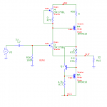
I just wanted to share this unit gain headphone amp circuit I designed and built it on Sunday.
So far it has exemplary performance and specs considering its simplicity, the built version exceeded my expectations:
Even thought I show a cap in the circuit, if the JFET's are matched the circuit is DC coupled input to output. I built 2 channels and 1 channel has 4mV DC offset andthe other has an 3.4mV DC output offset
The frequency responce is crazy I measured the responce to be almost perfectly flat with 0dB from 10Hz to 1MHz into a 33R resistor.
The specific JFETs isn't critical as long as IDSS is greater than 3mA and they are matched. I simulated with 2sk170GR, 2sk246GR/BL but I built it with 2sk117Y's (the model of the 2SK117 wasn't good).
The output bias current it set by 0.65/R75+R76, in the built version I went with R75 and R76 5R and R50 10R so it didn't run too hot.
I put it in a box last night and listening to Leonard Cohen with it now.
Have to give credit to Nelson Pass for his constant current stage and Erno Borbely for inspiration.
Cheers
Tim
Attachments
The positive power supply rail is named "VEE" and the negative power supply rail is named "VCC" ??
Most folks do it the other way.
edit- also you might want to call out a specific part number for Q1. Perhaps the MPS8599?
I did indeed mix up my supply notations, sorry about that.
The VEE supply I went with +12V and VCC -12V.
For Q1 I used a BC557 but I am pretty sure most jelly bean small signal PNP bjt's will do.
Cheers
Tim
Measurements
After listening to the amp for a week I thought I should make some distortion and square wave measurements.
First the distortion measurements.
The equipment used is an m-audio FireWire 410 on its rear line terminals. Levels calibrated against my DER EE DE-5203 true rms dmm.
Software used is the Visual Analyzer v.2014.
All measurements were done at 1kHz
Unloaded at 0.969vrms 0.0034% THD
25R load 0.960vrms 0.0034%
10R load the signal clipped about 2% THD
Reset the input level to Limit the current to 120mA into 10R so 1.2Vp or 0.846Vrms.
Unloaded 0.846Vrms 0.0034% THD
10R load 0.827 Vrms 0.021% THD
0.115% THD @ 0.87Vrms 10R
The harmonic content was predominantly 2nd.
I then measured the sound cards own output and it measured 0.0034%.
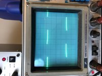
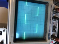
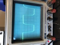
Now the square wave measurements.
Equipment used is a kenwood ag-203 source and an Iwatsu 100MHz analog scope.
First image is at 1kHz 0.5v/dev
Second is at 10kHz
Third at 100kHz
After taking the photos I then check the output of the ag-203 and they were exactly the same.
After listening to the amp for a week I thought I should make some distortion and square wave measurements.
First the distortion measurements.
The equipment used is an m-audio FireWire 410 on its rear line terminals. Levels calibrated against my DER EE DE-5203 true rms dmm.
Software used is the Visual Analyzer v.2014.
All measurements were done at 1kHz
Unloaded at 0.969vrms 0.0034% THD
25R load 0.960vrms 0.0034%
10R load the signal clipped about 2% THD
Reset the input level to Limit the current to 120mA into 10R so 1.2Vp or 0.846Vrms.
Unloaded 0.846Vrms 0.0034% THD
10R load 0.827 Vrms 0.021% THD
0.115% THD @ 0.87Vrms 10R
The harmonic content was predominantly 2nd.
I then measured the sound cards own output and it measured 0.0034%.
Now the square wave measurements.
Equipment used is a kenwood ag-203 source and an Iwatsu 100MHz analog scope.
First image is at 1kHz 0.5v/dev
Second is at 10kHz
Third at 100kHz
After taking the photos I then check the output of the ag-203 and they were exactly the same.
Attachments
Neat design, TimS.
Do you have photos of the amp to share?
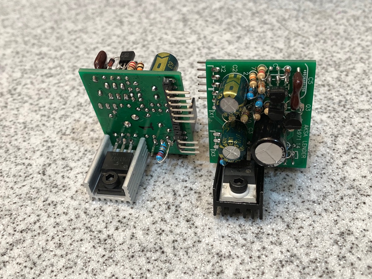
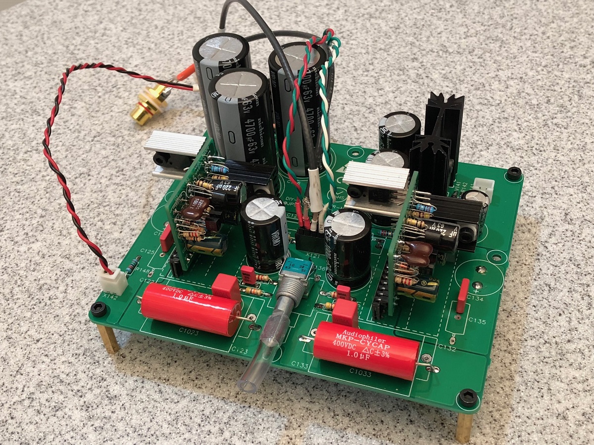
Although 5 actives is not exactly simple, I also have a 5 actives headphone amp based on Aksa Lender preamp and it doesn't uses any 2Sk170 JFETs. Not DC coupled output, but then it has advantage of single rail. Still 5 actives and very similar low THD figures and dominant H2 and lower H3, and has gain.
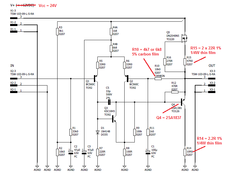
More info here
Aksa Lender HPA
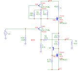
The amp core looks like this:
Which plugs into this for supporting PSU and input/output caps:
Do you have photos of the amp to share?
Although 5 actives is not exactly simple, I also have a 5 actives headphone amp based on Aksa Lender preamp and it doesn't uses any 2Sk170 JFETs. Not DC coupled output, but then it has advantage of single rail. Still 5 actives and very similar low THD figures and dominant H2 and lower H3, and has gain.
More info here
Aksa Lender HPA
The amp core looks like this:
Which plugs into this for supporting PSU and input/output caps:
Last edited:
Hi xrk971
The whole point why I shared this design is because it is DC coupled, as well as low distortion and wide bandwidth, with only 5 parts! Usually with simple designs I would add an integrator servo to remove output offsets (I really dislike output electrolytics).
Sure I used unobtainium (the 2sk170/2sk117's) in my design and not everybody has them in their part box but the design sims ok with BF265B, which are still currently sold at element14, just buy a bunch and match them.
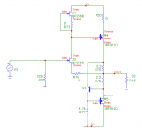
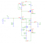
When I designed this circuit I didn't need gain (I have just got a Dragonfly Black for work listening and I wanted to see if it sounded better with an external amp) but it doesn't mean the circuit can't have gain while being DC coupled (second image). R81 could be a 1k pot to zero the last millivolts since this will have a larger DC offset like about 30mV.
I am shy about sharing actual pictures of the circuit since it was both a prototype that became the final design built in ugly style and I have hidden it in a nice box. It is nowhere as nice as the Aksa Lender PCB's.
Cheers
Tim
The whole point why I shared this design is because it is DC coupled, as well as low distortion and wide bandwidth, with only 5 parts! Usually with simple designs I would add an integrator servo to remove output offsets (I really dislike output electrolytics).
Sure I used unobtainium (the 2sk170/2sk117's) in my design and not everybody has them in their part box but the design sims ok with BF265B, which are still currently sold at element14, just buy a bunch and match them.
When I designed this circuit I didn't need gain (I have just got a Dragonfly Black for work listening and I wanted to see if it sounded better with an external amp) but it doesn't mean the circuit can't have gain while being DC coupled (second image). R81 could be a 1k pot to zero the last millivolts since this will have a larger DC offset like about 30mV.
I am shy about sharing actual pictures of the circuit since it was both a prototype that became the final design built in ugly style and I have hidden it in a nice box. It is nowhere as nice as the Aksa Lender PCB's.
Cheers
Tim
Attachments
Member
Joined 2009
Paid Member
The same Aksa Lender front end topology was applied to a dual rail output with Aleph CCS and PMOS output without any coupling caps as a power amp and it maintains 0 to 10mV DC offset from cold to hot without a nulling opamp. This is the Alpha amp. Now I am thinking an Alpha headphone amp version might be pretty interesting, say with IRF610 and IRF9610.
I could LTspice this and see what it looks like.
I could LTspice this and see what it looks like.
Hi Tim,
Will .25W resistors work in all locations or should R50, R75 and R76 be higher wattage resistors?
Thanks.
I am going to go through this in detail for anybody who wants to use different values for R50, R75 and R76. But the quick answer is 0.25 is fine for R75 and R76 but R50 should be 0.5W.
If you are using 2.2R as R75 and R76 then a constand current of about 0.7V / (2.2 + 2.2) = 0.16A running through them.
The power disipation for each resistor is 0.16A*0.16A*2.2R = 56mW
so a 0.25W resistor is fine for R75 and R76.
Power disipation for R50 is a little tricker:
Without a signal the current through R50 is the same as R75 and R76 which is 0.16A but during full output swing the amp can deliver twice the current or an additional 0.16A Peak or 0.16 * 0.707 = 0.113A rms giving a total RMS current of 0.16+0.113 = 0.273A rms.
The power disipated in R50 is 0.273*.0.273*5R = 0.372W, so I would go for 0.5W or since R50 isn't critical I would make it 4.4R by doubling up the resistors used for R75 and R76.
Cheers
Tim
You could try to split the r77 (to 2 x 2k4) and bootstrap it from the output with a 100-220uF cap.
You know what that works well I just tried it and it halves the simulated distortion figure.
Though I have to admit when the simulated distortion figure of my original design got to 0.0006%THD just before clipping, for such a simple circuit, I got all excited and stopped there.
But yes a 0.0003% simulated THD is a good improvement.
I included the circuit I simulated below, with Q1 label turned on
 .
.Cheers
Tim
Attachments
I have taken the liberty of putting this in LTSPice with a few changes :
1) Use currently available devices (2SK209, 2SA1312, FQP3P20 which I have good experience with).
2) Fiddle with the current ratio by changing the values of the 2x 2R2 bias control resistors.
3) Increasing the values of the feedback resistor network (seems no need for high bias at the input stage).
4) Remove input coupling cap and adjust DC at the top JFET CCS.
Performance at 1kHz is indeed excellent, but distortion is quite a bit higher at higher frequencies.
Using the lower MOSFET to swing more current reduces THD.
But this may not necessarily sound good.
And hope I did not make any stupid mistakes.
Best regards,
Patrick
.
Attachments
... and increases the cost of heatsinks ......
Using the lower MOSFET to swing more current reduces THD.
...
- Home
- Amplifiers
- Headphone Systems
- Simple High Performing Headphone Amp