A couple more comments to the cirucit if I may :
(I shall use the component designations in post 8.)
1)
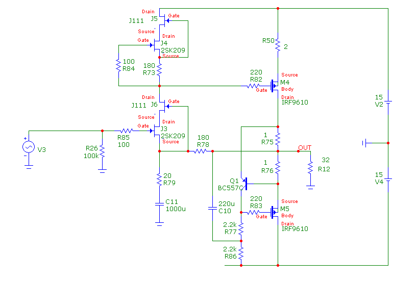
The voltage across the top CCS of the input stage J4/R73 is determined mostly by the Vgs of M4 under bias, plus I_M4*R50.
As such the top CCS would be starved of voltage headroom when low Vgs devices (e.g. lateral FETs) were used.
Most NJFETs like to have 4V Vds or so before they get to the "pentode" regime.
This limits the choice of MOSFETs to the like of IRFs or FQPs. Even 2SJ313 would be too low.
2)
Because of the above, J4 will not see the same Vds as J3, unless V+ is set deliberately low at 2x Vgs (M4), say around 9V, instead of say 15V
Most JFETs, including 2SK170 and 2SK209 (=2SK117), still has some dependency between Id and Vds.
Therefore J4, even when perfectly matched to J3 under the same Vds, will have a lower bias in circuit.
That implies DC input coupling always requires trimming.
And when that is the case anyway, there is no need to match J4 and J3.
One only need to make sure that J4 has a similar or larger Idss than J3.
And then R73 can be used to set the output DC to 0 while input is DC coupled.
It would be a real pity not to DC couple at the input, IMHO.
Patrick
(I shall use the component designations in post 8.)
1)
The voltage across the top CCS of the input stage J4/R73 is determined mostly by the Vgs of M4 under bias, plus I_M4*R50.
As such the top CCS would be starved of voltage headroom when low Vgs devices (e.g. lateral FETs) were used.
Most NJFETs like to have 4V Vds or so before they get to the "pentode" regime.
This limits the choice of MOSFETs to the like of IRFs or FQPs. Even 2SJ313 would be too low.
2)
Because of the above, J4 will not see the same Vds as J3, unless V+ is set deliberately low at 2x Vgs (M4), say around 9V, instead of say 15V
Most JFETs, including 2SK170 and 2SK209 (=2SK117), still has some dependency between Id and Vds.
Therefore J4, even when perfectly matched to J3 under the same Vds, will have a lower bias in circuit.
That implies DC input coupling always requires trimming.
And when that is the case anyway, there is no need to match J4 and J3.
One only need to make sure that J4 has a similar or larger Idss than J3.
And then R73 can be used to set the output DC to 0 while input is DC coupled.
It would be a real pity not to DC couple at the input, IMHO.
Patrick
A couple more comments to the cirucit if I may :
(I shall use the component designations in post 8.)
1)
The voltage across the top CCS of the input stage J4/R73 is determined mostly by the Vgs of M4 under bias, plus I_M4*R50.
As such the top CCS would be starved of voltage headroom when low Vgs devices (e.g. lateral FETs) were used.
Most NJFETs like to have 4V Vds or so before they get to the "pentode" regime.
This limits the choice of MOSFETs to the like of IRFs or FQPs. Even 2SJ313 would be too low.
2)
Because of the above, J4 will not see the same Vds as J3, unless V+ is set deliberately low at 2x Vgs (M4), say around 9V, instead of say 15V
Most JFETs, including 2SK170 and 2SK209 (=2SK117), still has some dependency between Id and Vds.
Therefore J4, even when perfectly matched to J3 under the same Vds, will have a lower bias in circuit.
That implies DC input coupling always requires trimming.
And when that is the case anyway, there is no need to match J4 and J3.
One only need to make sure that J4 has a similar or larger Idss than J3.
And then R73 can be used to set the output DC to 0 while input is DC coupled.
It would be a real pity not to DC couple at the input, IMHO.
Patrick
Hi Patrick
Constructive criticism is always appreciated.
1) I totally agree lateral and low Vgs MOSFETS will not work, but this still leaves a large number of devices to choose from, though it should have a low input capacitance and high transconductance.
2)This is indeed an effect but it isn't the main reason for having to trim the circuit. From testing in sim and building my prototype this effect causes an output change only in the mV's.
This could be improved by cascoding J3 and J4 , to keep there Vds's constant and equal. I am thing depletion mode mosfets but then it wouldn't be a simple circuit anymore.
The main problem, and I feel very stupid for not seeing it, the main issue is R79 going to GND!!.
In my original circuit, the setup for J4 is that it sets a bias current where the Voltage at the gate is equal the voltage at its source and through matching it is setting a bias current through J3, where the voltage at the gate is the voltage at its source and since the source it connected to the output then the voltage at the J3's gate is the voltage at the amplifiers output. If you then add a source resistor to J4 then the exact same source resistor has to be added to J3, but it can only connected to the amp output only!!
So how to we add gain? We put back R79 but we can't allow bias current to flow through it and the simplest way to do this is, I hate to say it, add a cap!! but it would still be dc coupled input to output.
We could still trim but the output offset will drift with temp and supply voltage and I am sure it kills its PSRR so I wouldn't recommend it at all.
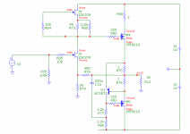
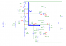
I also sim'ed your version of the circuit (attachment 1). I increased the output bias current and added boot strapping, put matching resistors for R75 and R76. (The asymetrical resistors allowed lower static bias but additional distortion when the output current started getting high).
On the sim I was getting 0.003% distortion swinging +/- 10V output into 32R at 1kHz and then again 0.030% distortion at 10kHz. I use microcap and I am not good at ltspice and it wouldn't load your mosfet model, so I stayed with the IRF9610, but the JFET model was fine.
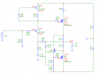
Attachment 2 shows how you circuit with gain should be done with an untrimmed 3mV output and a lower 0.002% distortion at 1kHz.
Cheers
Tim
Attachments
Tim,
Was never meant to criticise. Just intended to add a few remarks.
And it is a clever little circuit, so many congratulations.
The distortion numbers corresponds to those of my Spice results with the lower bias and no bootstrap.
So they more of less agree.
I have no problems trimming DC in my model.
(As you can tell from the different values of the JFET source resistors).
I also think equal current sharing is better.
But it is easy to try various ratio, and only listening will tell what sounds best.
I always have a gain of 10 because I use crossfeed upfront which sttenuates the input by -10dB.
But it just sounds so much more natural.
I suggest you try the Fairchild MOSFETs.
I like them better than the IRFs in the F5-HA.
Cheers,
Patrick
So after all this discussion back and forth between Tim and EUVL, is building the OP's circuit in the first post a total waste of time, or not??
Being such a simple circuit, I had already ordered all most of the parts from Mouser only to find out the circuit can be "improved" by Patrick's suggestions and simulations.
Personally, I'm not interested in a circuit with a gain of 10 with most devices outputting 2V or more, nor am I interested in circuit which uses "crossfeed" upfront as noted in post #24.
A clean sounding, low gain circuit works for me every time.
Tim,
Was never meant to criticise. Just intended to add a few remarks.
And it is a clever little circuit, so many congratulations.
The distortion numbers corresponds to those of my Spice results with the lower bias and no bootstrap.
So they more of less agree.
I have no problems trimming DC in my model.
(As you can tell from the different values of the JFET source resistors).
I also think equal current sharing is better.
But it is easy to try various ratio, and only listening will tell what sounds best.
I always have a gain of 10 because I use crossfeed upfront which sttenuates the input by -10dB.
But it just sounds so much more natural.
I suggest you try the Fairchild MOSFETs.
I like them better than the IRFs in the F5-HA.
Cheers,
Patrick
Thank you for your compliments.
This was just to be a weekend project, who's sim'ed performance surprised me enough to use some of my dwindling small supply of Toshiba JFET's, and the built performance surprised me enough that I thought I will share.
I will try the Fairchild devices, once I fine a spice model that works with microcap. The 2SK209's though are great I will look at getting some for future projects, its a pity about the size though.
I happen to have 100 BF256B's, that I brough for future RF projects, I will match them this weekend and build a prototype, of a more accessable version, to test for peoples interest.
I also want to purchase some depletion mode mosfets to add cascoding to the JFET's, to stabilise their Vds's, to hopefully lower distortion and to increase voltage handling.
I will also need to find spice models for them too.
Finally I already know of a way to remove the capacitor in the feedback network though it will require doubling the part count, so it would become a lot less simple but even more capable. But if it was implemented in more available and cheaper JFET's it might be worth it.
So if you or anybody else are interested into hacking this basic design into a balanced DC coupled capacitor-less, possibly lower distortion headphone amp, let me know.
Cheers
Tim
So after all this discussion back and forth between Tim and EUVL, is building the OP's circuit in the first post a total waste of time, or not??
Being such a simple circuit, I had already ordered all most of the parts from Mouser only to find out the circuit can be "improved" by Patrick's suggestions and simulations.
Personally, I'm not interested in a circuit with a gain of 10 with most devices outputting 2V or more, nor am I interested in circuit which uses "crossfeed" upfront as noted in post #24.
A clean sounding, low gain circuit works for me every time.
Guess my question wasn't worthy of a reply.

That's okay...I think I'll save my components for another project on another day.
Continue on gentlemen with your improvements for this ciruit.
Guess my question wasn't worthy of a reply.
That's okay...I think I'll save my components for another project on another day.
Continue on gentlemen with your improvements for this ciruit.
I am sorry I completely missed your post in my discussions with Patrick.
The the unity gain design in the very first post works great, I use it every day. Since i have built it the output offset is still in the 1-3mV range which is perfectly fine into headphones.
Last night I added a gate resistor on J3 and a 2k2 220pF input low pass filter but for no real reason rather that just in case, though it can't do a 1MHz square wave anymore
As Patrick pointed out there is the 2SK209 as a currently available SMD equivalent to the 2SK117Y's I actually used.
Cheers
Tim
Hi TimS, I´m collecting parts to build the buffer. On post #8 You mention BF265B and BF256B says the first schematic. On post #26, BF256B, which part should I buy? Do you have a schematic for power supply? I like your project, thank you!
Sorry my typo the part is BF256B I havn't actually tested the circuit but the simulation works OK but not as good as a 2SK170 or 2SK209 (2SK117).
I know I promised I would match and test some, but I got distracted this weekend.
Cheers
Tim
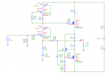
I simulated the cascode version of the 2SK209 amp with gain.
It fixes the issue with offset changing with supply voltage. It doesn't improve performace otherwise, probably the J111's own transconductance is quite low so doesn't add too much to the open loop gain.
Cheers
Tim
It fixes the issue with offset changing with supply voltage. It doesn't improve performace otherwise, probably the J111's own transconductance is quite low so doesn't add too much to the open loop gain.
Cheers
Tim
Attachments
IMHO you should consider what addition really makes a sonic difference, instead of chasing THD numbers.
Compared to post #1, it is not so simple anymore.
Cheers,
Patrick
All True
As a single ended headphone amp I have stopped at my first design, but I am thinking ahead to my next designs and I wanted to see what cascoding with the J111 was like.
The advantage, of reducing the output offset variablility to the supply voltage, is improved PSRR.
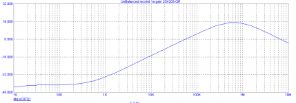
The first graph is of the PSRR of the cascoded version and the second is without. The third is the PSRR of my original design which has decient PSRR.
Cheers
Tim
Attachments
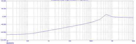
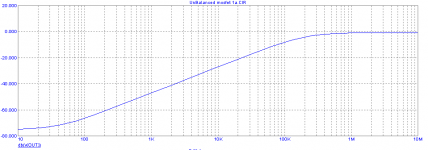
take your second graph, the non-cascode version; the knee is only c 300hz; so adding an RC filtering to the raw supply with a f-3db of ~300Hz means, the PSRR to raw supply is flat, & that's pretty easily done - 1ohm/470uF close enough; scale either component to suit, or go further: 1ohm/1000uF puts such things beyond contention. Two cheap resistors, two cheap caps, one raw supply - great PSRR and enhanced channel separation, fwiw; K.I.S.S.
I think your simple/sufficient approach to such an amp is a very elegant solution!
I think your simple/sufficient approach to such an amp is a very elegant solution!
Last edited:
low noise PSU
When JE1973 asked me about the PSU schematic, I really didn't have a plan I was running it off my lab PSU, I thought I would just suggest the usual LM317T and LM337T but then I remembered that the LM317 is noisy so I performed a little research and there are plenty of low noise designs out there.
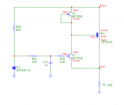
Then I had a brain storm, this thread is about a DC coupled JFET amplifier so why don't I use it as a DC amplifier ie a voltage regulator but I would use the more available (ie I have plenty) BF265B's. I would also just use a zener as a reference but with the JFET high input impedance I could use a large resistance and high quality capacitor RC filter to get rid of its noise.
So I matched a pair of BF265B's and built a pair of the circuits below.
Measurements:
- The supply voltage needs to be about 7V higher than the output voltage, so not particularly efficient.
- The output impedance is about 0.2R. I switched from 200R to 100R loads and the output changed 10mV, so not too bad.
- The voltage difference between the zener and the output is 30mV. Since I built this circuit twice I got about the same result which I think is fine for a PSU (better than the zener voltage) and the 30mV difference doesn't change much over time.
- Noise, I couldn't measure any using my scope I might try using my sound card later to better quantify this.
Last night I was running the lab PSU through a pair of these regulators and then into my original design headphone amp. I think it sounded better, low level detail became clearer.
My theory is the output impedance and so noise stays low across the audio range compaired to my lab psu.
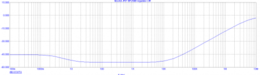
I don't have a suitably sized transformer so I can't check for ripple performance, but looking at the sim's the PSRR (2nd attached) is 54dB at 50/60Hz, so maybe it will need some preregulation or maybe cascoding of the JFET's, we shall see how that goes.
Cheers
Tim
Hi TimS, I´m collecting parts to build the buffer. On post #8 You mention BF265B and BF256B says the first schematic. On post #26, BF256B, which part should I buy? Do you have a schematic for power supply? I like your project, thank you!
When JE1973 asked me about the PSU schematic, I really didn't have a plan I was running it off my lab PSU, I thought I would just suggest the usual LM317T and LM337T but then I remembered that the LM317 is noisy so I performed a little research and there are plenty of low noise designs out there.
Then I had a brain storm, this thread is about a DC coupled JFET amplifier so why don't I use it as a DC amplifier ie a voltage regulator but I would use the more available (ie I have plenty) BF265B's. I would also just use a zener as a reference but with the JFET high input impedance I could use a large resistance and high quality capacitor RC filter to get rid of its noise.
So I matched a pair of BF265B's and built a pair of the circuits below.
Measurements:
- The supply voltage needs to be about 7V higher than the output voltage, so not particularly efficient.
- The output impedance is about 0.2R. I switched from 200R to 100R loads and the output changed 10mV, so not too bad.
- The voltage difference between the zener and the output is 30mV. Since I built this circuit twice I got about the same result which I think is fine for a PSU (better than the zener voltage) and the 30mV difference doesn't change much over time.
- Noise, I couldn't measure any using my scope I might try using my sound card later to better quantify this.
Last night I was running the lab PSU through a pair of these regulators and then into my original design headphone amp. I think it sounded better, low level detail became clearer.
My theory is the output impedance and so noise stays low across the audio range compaired to my lab psu.
I don't have a suitably sized transformer so I can't check for ripple performance, but looking at the sim's the PSRR (2nd attached) is 54dB at 50/60Hz, so maybe it will need some preregulation or maybe cascoding of the JFET's, we shall see how that goes.
Cheers
Tim
Attachments
This has a -0.461v DC offset in the LTSpice sim. It works well otherwise - how do you get rid of the offset without adding an input cap and bias network on the gate of J3?
The crux of this trick is J4 and R73 setting an Id where J4's gate voltage V1a (on drawing below) is equal to the voltage at V2a, since V1a and V2a are effectively connected.
Since J3 is matched to J4 and R73 is equal to R78, and the Id is the same through both JFETs then the voltage at V2b is equal to the J3's V1b gate voltage.
This all sounds great except for one thing the Id for any Vgs varies with Vds, especially with low transconductance JFETs. This is where the cascode comes in, it keeps the JFET's Vds the same so the offset doesn't change with the supply voltage.
If you are seeing an offset then one of 3 things:
R73 is not equal R78
or J3 is not matched to J4
or R79 is connected directly to GND
If R79 is connected directly to GND (ie no C11) then the current through R78 is not equal to the current through R73. R73 should approximatly be equal to R79 in parallel with R78 with some 'trimming'. In this case the parts matching is also less critical.
Cheers
Tim
Attachments
- Home
- Amplifiers
- Headphone Systems
- Simple High Performing Headphone Amp