Distortion measurements still haven't happened, but the headphone amp made a trip to Burning Amp 2018, powered by a bench supply. I used my AKG 240 Studio headphones for the demo. The final version of the amp will be powered by a hefty 19V laptop adapter, with a discrete DC-DC converter to provide the negative supplies. I only need 5V RMS, 7V peak to provide earsplitting volume (0.5W RMS), so a supply rail diet will make heat sinking much more simple.
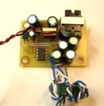
After some initial hiccups, the DC-DC converter is humming along nicely on my bench.
After some initial hiccups, the DC-DC converter is humming along nicely on my bench.
Uh-Oh. Ever heard of a can of worms?The final version of the amp will be powered by a hefty 19V laptop adapter, with a discrete DC-DC converter to provide the negative supplies.
You may have all kinds of fun with ground loops and EMC there, depending on how the notebook power supply is built (they vary widely) and how good your DC/DC layout is. The CD player you mentioned earlier seems to be an IEC Class I device (why do people do this in consumer audio? WHY?), don't be surprised if you encounter trouble with unwanted noises. (Same as an ordinary PC basically.)
Assuming you can afford it in terms of space, a conventional split secondary transformer supply (preferably with a shield winding if beyond 20-30 VA) followed by some capacitance multipliers would be a lot less problematic and more robust. Efficiency actually is not that bad given a good-quality transformer, maybe some Schottky rectifiers and a moderate (but still adequate) dropout on the cap multipliers. Nothing beats a conventional transformer in terms of isolation from mains and PE.
Last edited:
Nothing beats a conventional transformer in terms of isolation from mains and PE.
Batteries do a pretty good job too. When I listen to my battery powered O2 headphone amplifier, there is no mains hum at all. Even when I crank the volume control to maximum.
OK, so we'll assume that your DC/DC should be fine then ") - but how well do you know the 19V supply (which I assume is an off-the-shelf part)? What you want is a mains filter going to PE (I assume "hefty" means >75 W?), a transformer with shield winding, and not an awful lot more than maybe a kOhm and something nF-ish between PE and secondary-side ground. Copious amounts of common-mode chokes never hurt, but I guess you know that...
- but how well do you know the 19V supply (which I assume is an off-the-shelf part)? What you want is a mains filter going to PE (I assume "hefty" means >75 W?), a transformer with shield winding, and not an awful lot more than maybe a kOhm and something nF-ish between PE and secondary-side ground. Copious amounts of common-mode chokes never hurt, but I guess you know that...
I still don't know how much I'd trust something like this as an audio supply, but it should at least work OK.
- but how well do you know the 19V supply (which I assume is an off-the-shelf part)? What you want is a mains filter going to PE (I assume "hefty" means >75 W?), a transformer with shield winding, and not an awful lot more than maybe a kOhm and something nF-ish between PE and secondary-side ground. Copious amounts of common-mode chokes never hurt, but I guess you know that...I still don't know how much I'd trust something like this as an audio supply, but it should at least work OK.
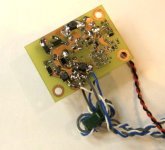
Here's the discrete DC-DC I'll be using to power headphone amp negative supplies. I used an LMC555 timer as controller because it was readily at hand, but there are some buck controllers from TI for automotive apps that drive a P-channel fet which could possibly be persuaded to work in invering flyback mode. Don't know about y'all, but I dislike having a bunch of single-purpose chips floating around in my inventory...
Attachments
The bias current for each side of the amp was slinmed down to 150 mA/side .
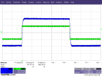
Shown are the square wave rise/fall times while driven by a function generator with 50 ohm output impedance - the amp is still quite zippy, but now prone to a little overshoot. A session with the gain-phase analyzer will help fix that. The analyzer I'm using actually has 5 MHz capability, so I should be able to directly see the phase margin at crossover.
Shown are the square wave rise/fall times while driven by a function generator with 50 ohm output impedance - the amp is still quite zippy, but now prone to a little overshoot. A session with the gain-phase analyzer will help fix that. The analyzer I'm using actually has 5 MHz capability, so I should be able to directly see the phase margin at crossover.
Attachments
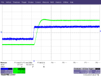
Looks like ~350 nsec 10-90 risetime so ~1MHz bandwidth at closed loop gain of 10.5X.
BTW I once copied the equations out of this paper and plotted a curve, see below. Naturally a number of assumptions are made when deriving the equations; you can decide whether the assumptions are reasonable or ridiculous.
_
BTW I once copied the equations out of this paper and plotted a curve, see below. Naturally a number of assumptions are made when deriving the equations; you can decide whether the assumptions are reasonable or ridiculous.
_
Attachments
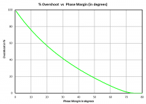
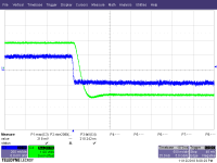
Sure but why not have a little fun with predictions too? The fall time plot seems to have an amplitude of 15 ticks (1 tick = 0.2 volts) and an overshoot of 1 tick. So that's about 6.7% overshoot.
Running through the equations in the .pdf which generated the green curve, we find that 6.7% overshoot corresponds to a damping factor zeta=0.655 and a phase margin of 62.5 degrees.
Won't it be delightful if the gain-phase analyzer gives the very same answer, at much greater expense and requiring much more human effort?
My idea of fun is not groping around in the dark trying to juggle 3 sets of poles plus a couple of zeroes. I will be making the investment for a G-P analyzer in the near future, most likely an HP4194A, which also doubles as an impedance analyzer. Both impedance and G_P functions go out to 40 MHz.
Right now, I'm using the Venable G-P analyzer we have at work, which has 5 MHz capability and costs me nothing.
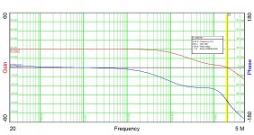
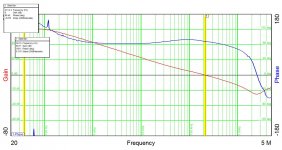
The first scan I made with original compensation had practically no phase margin and crossed over way too high, directly at odds with the relatively benign-looking time domain response. This may be possibly be due to the LP introduced by the input mosfet pair gate and Miller capacitance and a limited impedance input source. Anyway, here's what I have now after a fair amount of twiddling. The compensation values I'm using now are in the same ballpark as the values I originally used in my simulation to stabilize the design. I'll do the time domain response when I get a chance. I'd like to twiddle the compensation a bit more to get a more benign crossover slope, but 70 degrees of phase margin is not too shabby.
Right now, I'm using the Venable G-P analyzer we have at work, which has 5 MHz capability and costs me nothing.
The first scan I made with original compensation had practically no phase margin and crossed over way too high, directly at odds with the relatively benign-looking time domain response. This may be possibly be due to the LP introduced by the input mosfet pair gate and Miller capacitance and a limited impedance input source. Anyway, here's what I have now after a fair amount of twiddling. The compensation values I'm using now are in the same ballpark as the values I originally used in my simulation to stabilize the design. I'll do the time domain response when I get a chance. I'd like to twiddle the compensation a bit more to get a more benign crossover slope, but 70 degrees of phase margin is not too shabby.
Attachments
Boy the HP4194A is a wonderful piece of gear! I hope you snag one that needs very little TLC and refurbishment before you can begin using it.
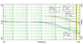
Looking at the blue "phase" line in the plot of #71, it seems to cross 45 degrees at 100 kHz. And that's likely to be a good approximation of the -3dB rolloff point. So we expect the 10%-90% risetime to be somewhere in the vicinity of 3.5 microseconds.
Gain of 10.5X ; bandwidth of 0.1MHz ; risetime of 3.5usec (predicted) ; phase margin of 70 degrees ; %overshoot of only 1.3% (predicted).
I did some work over the weekend, subbing 3X smaller fets in the output stage to move out the pole introduced by the gate + Miller capacitance. I went from IRF630/9630 t0 610/9610, reducing the capacitance by about a factor of 3.
I also reduced the rails to 16V from 19V, and upped the bias current to 200mA.
These changes allowed me to chip away at the compensation capacitors, increasing bandwidth while retaining (actually increasing) phase margin. The G-P scan also looks more "classic" as a result.
I want to try one more dodge before buttoning this thing up, tinkering with the stoppers on the input differential stage to perhaps push out the bandwidth a bit more.
The attached G-P plot shows a family of curves resulting from successive tinkering with the compensation values. The one of interest is plot #4 (grey/black). That compensation gets me 2.76 MHz gain crossover with 75 degrees phase margin.
Attachments
Here's the last pass of compensation tweaks. The amp is going home for some cleanup and installation in an enclosure.. The cases I have in mind for the finished unit will arrive early next week. I was thinking of routing out something nice in oak and sheet metal, but time is of the essence if I want to get this thing ready for Christmas.
I used ferrite beads on the gates of the input mosfet diff pair and got a little more bandwidth. Of the two gain phase curve sets shown, the one of interest is the orange/green pair, with a crossover frequency of 2.98 MHz and 62 degrees of phase margin. A second marker shows the frequency for 45 degrees of phase shift (313 kHz). The rise and fall times are a little under 1 usec.
One more thing I'll be trying over the Thanksgiving holiday is mating the amp with its negative supply DC-DC converter.
Attachments
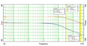
The plotted LF gain of +20dB suggests to me that this instrument has plotted the gain and phase of the control system with the loop closed. If were an open loop plot then the LF gain would be at least 30dB higher.
So, if this indeed IS a closed loop plot, you can't really read off the open loop gain margin or the open loop phase margin directly. You'll need to mathematically un-do the loop closure. And I doubt the instrument does this for you automatically, because if it did then the plotted LF gain would be more like +50dB.
So, if this indeed IS a closed loop plot, you can't really read off the open loop gain margin or the open loop phase margin directly. You'll need to mathematically un-do the loop closure. And I doubt the instrument does this for you automatically, because if it did then the plotted LF gain would be more like +50dB.
That open loop plot certainly shows enormous amounts of open loop phase margin, more than 90 degrees, at the crossover frequency of 200 kHz.
If I had an amplifier with that open loop plot, I would experiment with reducing the dominant pole compensation capacitor by a factor of about 5x. This would move the open loop crossover frequency up to about 1 MHz, where the open loop phase margin is still a quite respectable 75 degrees. More importantly it increases the amount of excess gain (a/k/a "the amount of feedback") by a factor of 5x, which gives a commensurate reduction in distortion. It also speeds up the square wave risetime response by the same factor of 5x.
There may be other not-quite-dominant poles and zeroes which begin to impact the open loop phase margin as you decrease the dominant pole compensation cap, so you may not be able to get the full 5x increase. But more bigger is more better, even if it's not 5x better.
Your amp has a gain of 10.5X and a -3dB bandwidth of 0.2 MHz, for a GBW product of 2.1 MHz. For purposes of comparison, the power amps in Bob Cordell's book have a GBW product of 16 MHz and the ones in Douglas Self's book have a GBW product of 20 MHz. So there is precedent for getting >2.1 MHz with thru hole parts and 2 layer PCBs and low priced non-military components. Even if the synthesized-SIT topology used here limits ultimate GBW, we'd hope to get at least half of what the books-for-beginners get, namely 8 MHz or so. In an optimistic and hopeful mood we could multiply 2.1 MHz by "almost 5x" and get 9 or 10 MHz which would be in that ballpark.
This project isn't dead, just sleeping a bit. For the sake of getting something out the door without a whole lot of complication, I opted for this simple single-ended design instead:
Simple Single-Ended Headphone Amp
The simpler design requires no parts matching and only needs a single +24V rail to run (no DC-DC converter!).
I'm looking at an option of this design that uses an Aleph-style modulated current source on top of the output stage rather than the complicated mirror scheme. This decouples the output biasing from the input stage tail current, and dramatically reduces the parts count. If I can gin up a modulated current source using a commercially available depletion mode mosfet, even better.
- Status
- This old topic is closed. If you want to reopen this topic, contact a moderator using the "Report Post" button.
- Home
- Amplifiers
- Headphone Systems
- Discrete Headphone Amp.