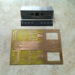
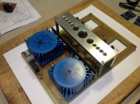
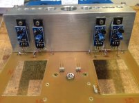
Completed the double rectifiers, to more insane rectifier assembly I ever did for just an headphone amp  , fully dual mono power supplies, bigger than some integrated we see on the market!
These rectifiers are big enough for a power amp Thanks Patrick, but I'm always serious when building something Now time to check all this, don't worry nothing is still soldered. First the power transformer primaries and secondaries, then the rectifier without the transformer, with just an ohm meter, then with a dual polarity, current limited external DC power supply, then the real thing all together, and finally I'll connect the +-15V regs. Better safe than sorry, and my board is still just a prototype...
, fully dual mono power supplies, bigger than some integrated we see on the market!These rectifiers are big enough for a power amp
Thanks Patrick, but I'm always serious when building something Now time to check all this, don't worry nothing is still soldered. First the power transformer primaries and secondaries, then the rectifier without the transformer, with just an ohm meter, then with a dual polarity, current limited external DC power supply, then the real thing all together, and finally I'll connect the +-15V regs. Better safe than sorry, and my board is still just a prototype...Attachments
Last edited:
But not every power amp has 150mA bias as well.
One could also use SBYV27-200 instead.
You might want to check this out :
http://www.diyaudio.com/forums/power-supplies/313202-quasimodo-results.html#post5206814
Patrick
One could also use SBYV27-200 instead.
You might want to check this out :
http://www.diyaudio.com/forums/power-supplies/313202-quasimodo-results.html#post5206814
Patrick
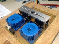
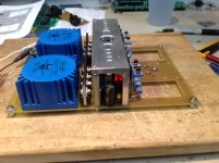
I usually build power amps with more than 1-2A bias Big Class-A, but I love Class-A headphone amps as well. My latest has 300ma bias per channel... I made a few fully discrete ones in Class-A: Borbely (Aural Audition commercial version clone), X5 fully discrete, including a discrete op-amp, the Salas DCB3, and a few others I cannot discuss Check the pictures...
Big Class-A, but I love Class-A headphone amps as well. My latest has 300ma bias per channel... I made a few fully discrete ones in Class-A: Borbely (Aural Audition commercial version clone), X5 fully discrete, including a discrete op-amp, the Salas DCB3, and a few others I cannot discuss Check the pictures...Attachments
Last edited:
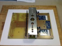
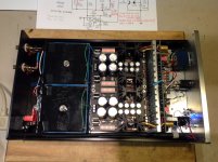
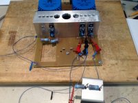
Half the work done, complete power supply is tested and assembly is all done...
With all the PCB real estate available, I couldn't resist and installed a CRC filter just afterthe rectifier bridges and power-on leds...
Both power supplies were tested under 150ma load, less than 4mvac ripple on each +-15V supplies.
With all the PCB real estate available, I couldn't resist and installed a CRC filter just afterthe rectifier bridges and power-on leds...
Both power supplies were tested under 150ma load, less than 4mvac ripple on each +-15V supplies.
Attachments
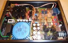
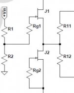
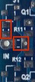
Hi Patrick. A little precision here, look at both inputs JFET and BJT. The instruction says to ommit R1,R2 if using the JFET, but the JFET input schematic still shows R1, R2, and on the PCB there are pads for 0603 (input) and 0805 (to gnd) size resistor, but without name.
Are we still using these two input resistors with the JFET input, and if yes what are the values? Thanks
SB
Are we still using these two input resistors with the JFET input, and if yes what are the values? Thanks
SB
Attachments
Last edited:
> but the JFET input schematic still shows R1, R2,
Those represents the source resistance and the input grounding resistor.
Forgot to chnage the resistor numbers from Spice model.
Sorry for that.
> and on the PCB there are pads for 0603 (input) and 0805 (to gnd) size resistor,
0603 (2x) are gate stoppers for J1 & J2. Use 220R.
The 0803 that you showed in the photo (on the top side) should be left open.
(Use 0805 0R there ONLY when NOT using J1,2.)
There is another resistor to Gnd at the bottom side of the input pin.
This is the input grounding resistor. Use 100k at that position.
They should be on the Bill of Materials.
> but without name.
PCB too small ......
Patrick
Nice progress Algar_emi! It’s going to be a superb build I’m sure.
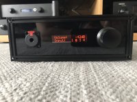
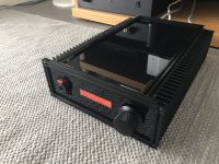
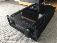
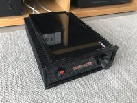
You got me inspired to finally update my front plate and the vol knob. I think the new knob is a bit too big and heavy - so still to do another update on that behalf.
You got me inspired to finally update my front plate and the vol knob. I think the new knob is a bit too big and heavy - so still to do another update on that behalf.
Attachments
-
 CA928AD0-0CA4-4204-96A8-77FA58933644.jpeg756.6 KB · Views: 330
 -
 9199B2B5-918D-4311-88C2-087B9E70D3B9.jpeg975.8 KB · Views: 284
 -
 938E8185-7A5B-4A0A-88CD-3A3B075C4411.jpeg850.5 KB · Views: 264
 -
 C8199CFD-562C-4CF1-B08B-5593F56A4C31.jpeg928.2 KB · Views: 293
 -
 602E3740-97E0-4887-B85B-353A9A567E82.jpeg888.8 KB · Views: 898
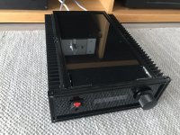
Wow, mine won't be so gourgeous , but I have a lot of amps, have to save somewhere
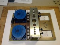
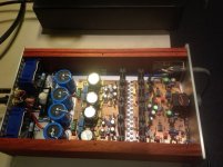
Both channels are now tested, working very nicely. Second channel DC offset is so low at less than 4mv (2.5mv under 33R load), that probably I won't bother trying to tune it to zero. Anyway without servo it will always fluctuate around 0mv anyway... Now time to assemble the protection PCB
Also check how the circuit is sensitive to +-15V exact value variation. Probably thanks to the CCS, not that much. Set one supply from +14.90 to +14.40, while keeping the other at -15.0V, and the DC offset didn't move. Excellent!
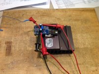
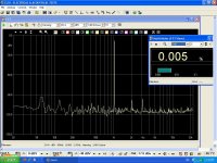
Here my first measurements, with lab power supply, and without enclosure...
All measurements done using a 33R resistor.
Gain: (Vin: 100mV, Vout: 10V) = 10X or 20dB
Vout max: 20Vp-p or 7.3Vac, that gives 1.6W
Vin max: 0.723V
BW (Ref 1Khz, Vout 1V): 3.1Mhz...
Noise (gnd input): < 1mv (THD graph showing noise floor close to -115dB
THD (Vout 1V): < 0.005% (limit of my equipment), see graph
Output DC offset: 2.5mv
, but I have a lot of amps, have to save somewhere Both channels are now tested, working very nicely. Second channel DC offset is so low at less than 4mv (2.5mv under 33R load), that probably I won't bother trying to tune it to zero. Anyway without servo it will always fluctuate around 0mv anyway... Now time to assemble the protection PCB
Also check how the circuit is sensitive to +-15V exact value variation. Probably thanks to the CCS, not that much. Set one supply from +14.90 to +14.40, while keeping the other at -15.0V, and the DC offset didn't move. Excellent!
Here my first measurements, with lab power supply, and without enclosure...
All measurements done using a 33R resistor.
Gain: (Vin: 100mV, Vout: 10V) = 10X or 20dB
Vout max: 20Vp-p or 7.3Vac, that gives 1.6W
Vin max: 0.723V
BW (Ref 1Khz, Vout 1V): 3.1Mhz...
Noise (gnd input): < 1mv (THD graph showing noise floor close to -115dB
THD (Vout 1V): < 0.005% (limit of my equipment), see graph
Output DC offset: 2.5mv
Attachments
Last edited:
Noise floor will go down with proper PSU and case.
Even as it is now, with the limit of your measuring equipment, you should be very pleased.
It will not shy from any commercial amps of any price.
And all that without global NFB.
Time to finish off and have a listen with a less expensive headphone.
(Should use SHPP with your reference phone.)
Patrick
Hi Patrick. I have problem with the SHPP leds, 0805 format. None of the Red, Green or Yellow turns on. I test all the leds with my DVM, diode mode, and they are working, but inside the circuit, they don't turn on when activated. I have
D1 (Red): channel fault
D3 (Grn): Power On
D6 (Yel): Delay
What led part number did you used, mine seem to be not of the correct voltage?
Thanks
SB
D1 (Red): channel fault
D3 (Grn): Power On
D6 (Yel): Delay
What led part number did you used, mine seem to be not of the correct voltage?
Thanks
SB
- Home
- Amplifiers
- Headphone Systems
- The Pioneer Super Linear Circuit