The gate-source voltage of the IRF520 and IRF510 will only be about 0.5 V different, the main reason you have 7 V at the MOSFET source is your supply voltage is 12 V rather than 9 V.
You need to increase R3 in proportion to the increase in supply voltage. Try using 1.5k or 2.2k instead of 1k.
You need to increase R3 in proportion to the increase in supply voltage. Try using 1.5k or 2.2k instead of 1k.
Attachments
I've now got the amp working using 12V and IRF510.
I used jfets which measure Vgs1.3 on my little component tester. It seems the Vgs has a big impact on the operating points of the circuit.
R3= 2.2kohm
R2= 220ohm
R4=20 ohm
On one channel I measure 2.3V across R4 and 2.7V on the other channel. Does this make any difference?
Also, the sound is very clear but it seems to be bright and not have as much bass as other circuits. Is this normal? Would increasing the output capacitor have an effect?
I'm using Audio Technica ATH M50, which are 33ohm.
Thanks again
Last edited:
Vgs needs to be similar for both channels, but it normally is. 2.3 V and 2.7 V seems a larger than usual variation, though it's usable. Your bias currents will be 2.3/20 115 mA and 2.7/20 135 mA.
33 ohms will give a -3 dB bass cutoff of 5 Hz with the 1000 uF capacitor. You shouldn't need a larger one, but it may be worth experimenting.
33 ohms will give a -3 dB bass cutoff of 5 Hz with the 1000 uF capacitor. You shouldn't need a larger one, but it may be worth experimenting.
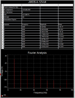
The distortion shown is at a very low output power though, just 0.5 mW into 32 ohms. I mean, yes that's close to typical listening levels but if you reported it as output power for 1% THD+N for example, it wouldn't look nearly as nice.
It is what it is, as I've always said about this circuit. A fair amount of (mostly second harmonic) distortion, and very little power supply ripple rejection, it won't be winning any contests for design elegance. Quick and dirty, sounds nice. No claim to anything else.
It is what it is, as I've always said about this circuit. A fair amount of (mostly second harmonic) distortion, and very little power supply ripple rejection, it won't be winning any contests for design elegance. Quick and dirty, sounds nice. No claim to anything else.
Last edited:
")
Farnell has many J113
https://uk.farnell.com/on-semiconductor/j113/transistor-jfet-n-to-92/dp/1017713
https://uk.farnell.com/on-semiconductor/j113/transistor-jfet-n-to-92/dp/1017713
As a side note, normally I would avoid using active parts marked as "designed for low level analogue switching, sample and hold circuits and chopper stabilized amplifiers." in an audio amplifier, since it implies the part was optimized for fast switching characteristics rather than low distortion or low noise.
However ... it's a JFET. The parts vary by transconductance and transfer characteristics and as far as I know there is no practical difference** between parts marked as "for audio" and those aimed at switching applications, this is chosen by looking at the device characteristics and marketing figuring out who is most likely to want it.
** Their could be tradeoffs at the silicon level, to tweak capacitance and noise, but I've used a few different types for phono stages, for example, as well as in different iterations of the J-Mo, and never noticed any difference in sound quality between the parts.
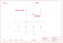
I think I will not simulate at 12 Volt.Hej Lineup, did you mean to simulate with 12 volts, as it says 9V?
But if I do, I will post the result here.
12 Volt simulation and adjust
See the first image.
I suggest changing R3 to 1.8k.
And replace R1 with two 15 Ohms resistors.
The gain of this circuit is around x4.
So the gain is more than the 9 Volt circuit.
The THD is acceptable.
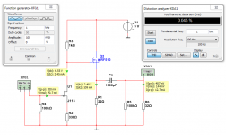
See the second image.
It shows that the distortion is mostly 2nd and 3rd harmonics.
See the first image.
I suggest changing R3 to 1.8k.
And replace R1 with two 15 Ohms resistors.
The gain of this circuit is around x4.
So the gain is more than the 9 Volt circuit.
The THD is acceptable.
See the second image.
It shows that the distortion is mostly 2nd and 3rd harmonics.
Attachments
- Home
- Amplifiers
- Headphone Systems
- JFET-MOSFET headphone amplifier J-Mo 3