I'm not 100% certain but it looks like the highest value they make as a mini, stereo, audio taper, pot is 20K.
The part no. is RK09712200MT.
The part no. is RK09712200MT.
Oh right, I forgot to mention - I removed the trestrict layer that you put around the heatsink lugs, so unless you put them back please isolate the FETs and regulator from the heatsink using a thermal pad.
Generally I think its better to ground the heatsinks and isolate the active devices.
I hope the way you have the layout - with a ground plane shared by all the returns - is okay. It should be satisfactory, but there is an argument for instead tying the signal returns from each channel together before connecting down to the main ground plane. This would be better, but given the particulars of the way you've arranged the components rather difficult to execute.
Final note there is less room between the heatsinks than I'd like, getting into the space between them will need some smallish fingers so plan the build carefully to do the hard to access parts first, before the heatsinks are added.
/R
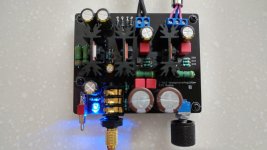
Working great.
I need more time for sound test, at least it is not burning.
It is not audible during music play, but there is small amount of hum in background. I need to fix it too.
Audible with Koss KSC35, inaudible with HD650.
I need more time for sound test, at least it is not burning.
It is not audible during music play, but there is small amount of hum in background. I need to fix it too.
Audible with Koss KSC35, inaudible with HD650.
Attachments
Last edited:
Nice work, Withmat!
This amp topology sounds great - one of the best. But it has no power supply ripple rejection capability. The PSU quality = amp quality. What is your PSU?
Use a DC-DC step up as it provides a built in CLC to remove mains 60Hz / 50Hz hum. The use a small mosfet cap Mx to knock hum by -50dB. Follow with simple CRCRC using 4700uF and 0.47R. You will then have a flat noise floor down to -130dB.
This is all built into the main board holding the two SE Class A daughterboards of my new Aksa Lender preamp/headphone amp. Look at schematic for main board and you will see Input is Dc from a smps.
His PSU is what is what you see built onto the board. It's all there right down to the diodes. LM7815 iirc, with dual CRC filter.
You are absolutely right about the circuit having zero PSRR - that's one of the things that keeps it off my list of favorites - but the LM7815 and filter caps should see to it that there is no ripple on the output, at least not audible, at least not in theory.
My concern is more the layout, the limited space meant the supply is placed right next to the input section, and everything is dumped to the common ground plane. Plenty of opportunity for noise pickup.
His PSU is what is what you see built onto the board. It's all there right down to the diodes. LM7815 iirc, with dual CRC filter.
You are absolutely right about the circuit having zero PSRR - that's one of the things that keeps it off my list of favorites - but the LM7815 and filter caps should see to it that there is no ripple on the output, at least not audible, at least not in theory.
My concern is more the layout, the limited space meant the supply is placed right next to the input section, and everything is dumped to the common ground plane. Plenty of opportunity for noise pickup.
Yes, it seems layout issue. My J-Mo3 still sounds great, no hum until midium volume - which is enough for HD650 also - but I think rectifier is too close to audio path. I will try with avalanche diode, and try another layout if avalanche diode does not help.
What I think for next PCB is deviding ground for ac and signal, and upgrade volume for 16mm or 27mm pots.
I won't use any kind of switching PSU, since PSRR of this circuit is almost zero, as Richard mentioned
Last edited:
I won't use any kind of switching PSU, since PSRR of this circuit is almost zero, as Richard mentioned
The SMPS puts the "mains" freq up to 400kHz (sometimes 1.2Mhz depending on SMPS) where it can be filtered steeply with a small CRC to basically zero. Do not "fear" SMPS for their noise if you properly use it to your advantage. 60Hz frequency is in audio band and much harder to eradicate. Think of it this way, by using a linear trafo/bridge/CRC/linear regulator you are trying to take 120VRMS noise source down uVrms levels at the very audible frequency of 60Hz/120Hz/180Hz (that's 10E-10 reduction a tall order). No matter how hard you try, can any linear regulator do much better than -80dB maybe -100dB? But if the switching frequency is 400kHz, you can be many octaves below and be able to apply easy and steep CRCRC or CLC filtering. Plus, the residual that isn't filtered cannot be heard.
Here is an example of the noise floor with DC SMPS cap Mx and CRC filter:
Last edited:
@withmatt
Note you can drive your boards from a DC voltage as is, with no modification needed whatsoever. The bridge recitifier now acts as a safety, it makes the power inputs unipolar which is a neat little feature.
This means you can sit back and experiment with external DC power supplies to your hearts content until you find something that works for you.
Last edited:
What a great headphone amplifier!!
J-MO = JFET + MOSFET
Come on, please tell me this is some kind of joke!
Come on, please tell me this is some kind of joke!
Well, I mean - err.. of course it is. Though the humor looks a bit dated now, the original circuit came out shortly before the album.
@Lineup
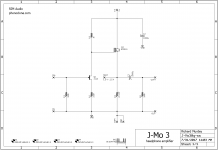
Yes, that's the final circuit schematic revision. The rest of the materials are attached.
Attachments
No, I really mean my positive words.Come on, please tell me this is some kind of joke!
For headphones amp we can make it simple but good working.
I like Keep It Simple, KIS, designs.
And RJM would not publish if it wasn't good.
I see there are followers that has further developed this concept in their circuits.
@rjm
Thanks man. Keep on your good works
")
What software is used for pcb and schematic?Well, I mean - err.. of course it is. Though the humor looks a bit dated now, the original circuit came out shortly before the album.
@Lineup
Yes, that's the final circuit schematic revision. The rest of the materials are attached.
- Home
- Amplifiers
- Headphone Systems
- JFET-MOSFET headphone amplifier J-Mo 3