I plan to disclose the complete circuitry and PCB layout information of the following CS6A4689 headphone amplifier evaluation board.
CSEVB6401R2 Product Brochure-15June2017-16
If you are interested to purchase a sample of it, do please drop me a message.
CSEVB6401R2 Product Brochure-15June2017-16
If you are interested to purchase a sample of it, do please drop me a message.
Last edited:
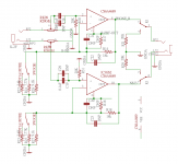
The core circuit is the CS6A4689 based hifi amplifier.
The feedback path will control the amplifier gain.
In this circuit, three different gains
1.3x 4x 9x
is obtained by the three way switch SW3G$1
Besides the amplifier gain, the input audio volume
is also controlled by a dual-band RK09, a 50Kohm
variable resistor.
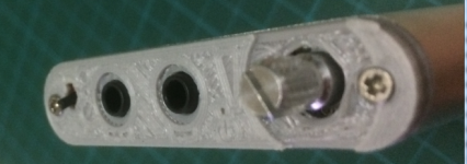
The output of the amplifier is connected to a 3.5mm jack
through relay K1. The control circuit of the relay will
be provided in the next post.
You may noticed that there are a lot of DNP components
which are provided to make the PCB layout to be able to adapt
to different component sizes, and also provided to allow
user to adjust the amplifier through beta-feedback circuit,
which will include the gain bandwidth, and tonal, etc.
In it's most pain form, the feedback path will just be
a simple resistor based voltage divider as shown in the
attached schematic.
Enjoy!
The feedback path will control the amplifier gain.
In this circuit, three different gains
1.3x 4x 9x
is obtained by the three way switch SW3G$1
Besides the amplifier gain, the input audio volume
is also controlled by a dual-band RK09, a 50Kohm
variable resistor.
The output of the amplifier is connected to a 3.5mm jack
through relay K1. The control circuit of the relay will
be provided in the next post.
You may noticed that there are a lot of DNP components
which are provided to make the PCB layout to be able to adapt
to different component sizes, and also provided to allow
user to adjust the amplifier through beta-feedback circuit,
which will include the gain bandwidth, and tonal, etc.
In it's most pain form, the feedback path will just be
a simple resistor based voltage divider as shown in the
attached schematic.
Enjoy!
Attachments
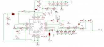
From a 3.7V Li-ion battery to +/-10V dual rail supply, we applied the CS7D651 DC-DC converter. A very low noise DC-DC converter with enough output current for the high performance CS6A4689 amplifier IC
Noted that a simple connection of the DC-DC output and the amplifier with do the job in raw.....but with power on pop....We shall show you how we resolve that problem in my next post
Noted that a simple connection of the DC-DC output and the amplifier with do the job in raw.....but with power on pop....We shall show you how we resolve that problem in my next post
Attachments
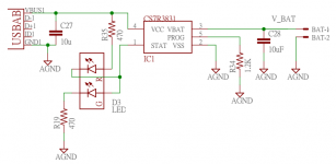
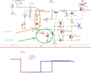
The start up pop sound is removed by two separate delay circuit
1. The power on delay circuit. After switching on, VSYS will increase
from zero to 3.7V (the Li-ion battery voltage). Which will charge up
C32 through R1. This charge up action will create a delay.
After the capacitor C32 is charged up to 0.7V, Q2 will conduct, which
in turn will turn on PMOS G1 and G2, and conduct the Li-ion battery power to VCC and power on the DC-DC converter, and all then the headphone amplifier IC.
2. The other delay circuit is the power on headphone isolation circuit.
At power on, the headphone is isolated from the amplifier through relay K1.
The relay K1 will keep turning on until the DC-DC power supply stable,
than it will be closed (K1 is a normal close relay) with the relay coil power being removed.
There are a few more tricks needed to create a high quality headphone amplifier which will be described in my next post.
Attachments
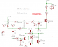
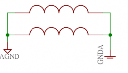
You might have noticed that the DC-DC converter, and all associated power circuitry use AGND,
While the power amplifier use GNDA
Ground isolation is one of the best technique to create a silent background...much higher signal to noise ratio can be achieved by this
simple circuit technique.
Knowing that the circuit cannot has two unrelated ground, they have to be connected, and this is achieved via ferrite bead. We shall use WE-CBF from Wurth Electronics, and two ferrite beads are added on the pcb, which has a physically separated ground plan for GNDA and AGND.
Attached is the last piece of schematic for this project.
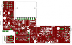
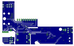
My next post will be about the pcb layout.
While the power amplifier use GNDA
Ground isolation is one of the best technique to create a silent background...much higher signal to noise ratio can be achieved by this
simple circuit technique.
Knowing that the circuit cannot has two unrelated ground, they have to be connected, and this is achieved via ferrite bead. We shall use WE-CBF from Wurth Electronics, and two ferrite beads are added on the pcb, which has a physically separated ground plan for GNDA and AGND.
Attached is the last piece of schematic for this project.
My next post will be about the pcb layout.
Attachments
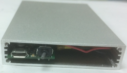
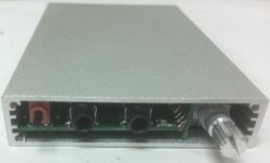
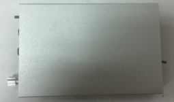
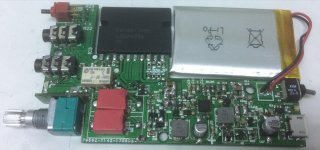
when we put everything together this is the final PCBA....a very compact working headphone that can fit into a slim excursion AL case.
1. Please note that the front and back side AL covers are leave out to show the inside.
2. This is a hand soldered sample, which you can obvious observe the poor soldering quantity. So...be minded with the very very poor soldering")
1. Please note that the front and back side AL covers are leave out to show the inside.
2. This is a hand soldered sample, which you can obvious observe the poor soldering quantity. So...be minded with the very very poor soldering
Attachments
Nice project!
Yeah, but it's going to be limited to the number of people that can solder all those microscopic SMDs onto the board.
No doubt those devices make for a nice compact board, but it limits the number of people who are able to build it...including myself.
If I can't purchase something like this already assembled, tested and ready-to-go, then I personally stay away from these "nightmare to assemble" SM designs.
Soldering SMD parts is not that difficult, it can be easily done with hot air gun or even a toaster
https://www.youtube.com/watch?v=2Z7nCAxS2Rg
https://www.youtube.com/watch?v=SN8fzpigTGM
The sample that we've built in house and has the photos posted in this thread are soldered with chipquik
http://www.mouser.hk/ProductDetail/Chip-Quik/SMD4300SNL10/?qs=sGAEpiMZZMsQWb9Zho8SKpiVtS3TQhIh
and an old toaster oven, just like that posted in youtube.
Of course, if you are interested to get a pcb with everything soldered on it,
do please let me know where I shall courier it to, and I shall quote to you.
Actually if you want all the components, and bare PCB, you can also contact me, and I shall quote to you about that too.
Hi Ammel68,
The gain of the amplifier is controlled by the negative feedback resistor pairs. The posted circuit has a 3 way switch connected to it, and hence makes it adjustable. The posted circuit has the gain to be adjustable between
1.3x 4x 9x
If you want 6dB, all you need to do is to change the feedback resistor values, and that will do.
some more details on the start up pop sound removal circuit, which also
give enough time for the DC-DC converter to settle. With refer to the attached figure, the key is to allow enough time between circuit being powered up (the blue signal), and the relay being released (it's an normal short relay). Adjusting the RC timing according to that label in the schematic will help to achieve the desired power up delay (and hence pop sound removal), and the wait time that you find flustrated.
give enough time for the DC-DC converter to settle. With refer to the attached figure, the key is to allow enough time between circuit being powered up (the blue signal), and the relay being released (it's an normal short relay). Adjusting the RC timing according to that label in the schematic will help to achieve the desired power up delay (and hence pop sound removal), and the wait time that you find flustrated.
Attachments
Hi Ammel68,
The posted circuit has the gain to be adjustable between
1.3x 4x 9x
If you want 6dB, all you need to do is to change the feedback resistor values, and that will do.
1.3x or 4x gain will work for me. How much for an assembled board to the U.S.?
Thanks.
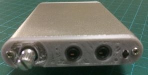
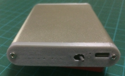
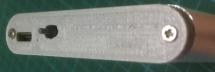
Changed to a round corner case, and 3D printed the front and back cover
Now the amplifier is running perfectly. The next step will be making a AL CNC front and back cover
Now the amplifier is running perfectly. The next step will be making a AL CNC front and back cover
Attachments
Thanks for your messages thuanth43, and ammel68.
Actually, I was wondering if I put this amplifier to Kickstart, will
you guys be my honored supporters? If that's the case, what price range will you be willing to pay for it? say, assembled PCB, and assembled PCB with CNC AL case. What about customerization, say using better quality input DC blocking capacitors, etc....
Thanks in advance for your inputs....
Cheers
- Status
- This old topic is closed. If you want to reopen this topic, contact a moderator using the "Report Post" button.
- Home
- Amplifiers
- Headphone Systems
- CS6A4689 Headphone amplifier project