Hi All,
Like some of you I followed with great interest the thread 'New Audio Op Amp - OPA1622' by TI’s Johnnc124. I wasn’t initially specifically interested by headamps but as the OPA1622 was simple to implement and was supposed to provide good results I decided to setup a project with it. More than building an headamp this project was aimed to confirm I could achieve designing a PCB with a CAD software and also soldering SMD devices, including ones in DFN or QFN package.
I’have finally been through all steps, I’m happy with the result (OPA1622 sounds very good !) and I’m now confident to move to projects that will require complicated PCB and good soldering capabilities.
Now, I have to finish assembly and testing of a Salas DGC3 in order to do some comparisons!
The main requirements for AmpCasq where :
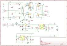
About the schematics:
Regulators:
Like some of you I followed with great interest the thread 'New Audio Op Amp - OPA1622' by TI’s Johnnc124. I wasn’t initially specifically interested by headamps but as the OPA1622 was simple to implement and was supposed to provide good results I decided to setup a project with it. More than building an headamp this project was aimed to confirm I could achieve designing a PCB with a CAD software and also soldering SMD devices, including ones in DFN or QFN package.
I’have finally been through all steps, I’m happy with the result (OPA1622 sounds very good !) and I’m now confident to move to projects that will require complicated PCB and good soldering capabilities.
Now, I have to finish assembly and testing of a Salas DGC3 in order to do some comparisons!
The main requirements for AmpCasq where :
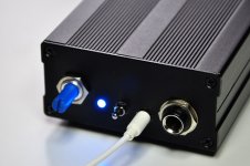
- It should stand in a small aluminum box, in order to sit on desk
- It should be powered by an AC adapter I had, which provided 17VDC
- It should have a volume control
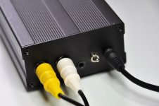
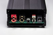
- It should have RCA and jack 3.5 inputs
- It should have jack 3.5 & 6.35 outputs
- It should allow me to experiment crossfeed
- Final price should stay under control
About the schematics:
Regulators:
Ampcasq was designed in September 2016, at this time LM27762 was announced but not available. So, I did stay with LM27761 for -5V and LP38798 for +5V; LP5907 was a bit short on current. The 7805 lifted by R17/R12 was added to limit LM27761 input voltage to 5.5V, its max value. 7805 allow Ampcasq to be powered by any DC source from 10V to 35V, 300mA max.
Power Input:
D1 to protect against bad connection.
D2, R23, R10, R11, C24 to manage the Enable pin of the OPA. Objective was to avoid noise in the can at power up/down. This partly works: mute the output when enable Low (<~0.8V) but can’t avoid noise in can when power supply capacitors are discharching and OPA1622's supply getting out of tolerance. On power off with SW1, OPA1622 is muted as C24 is quickly discharged through R23, D2 and SW1. D2 is a Schottky, not for speed but for low drop (Vf close to 0.3V).
Crossfeed:D2, R23, R10, R11, C24 to manage the Enable pin of the OPA. Objective was to avoid noise in the can at power up/down. This partly works: mute the output when enable Low (<~0.8V) but can’t avoid noise in can when power supply capacitors are discharching and OPA1622's supply getting out of tolerance. On power off with SW1, OPA1622 is muted as C24 is quickly discharged through R23, D2 and SW1. D2 is a Schottky, not for speed but for low drop (Vf close to 0.3V).
It is based on an Xen-Audio (EUVL) paper: Xen Audio cross feed.
There’re three positions for the switch: Low Xfeed – No Xfeed – High Xfeed. Low Xfeed is Ok, High is exaggerate: there’s too much bass boost. After some listening sessions I finally do not use the Xfeed.
Gain + outThere’re three positions for the switch: Low Xfeed – No Xfeed – High Xfeed. Low Xfeed is Ok, High is exaggerate: there’s too much bass boost. After some listening sessions I finally do not use the Xfeed.
Not much to say.
Attachments
Some pictures
It's mostly finished, but a (very) important thing is missing : a nice volume button")
It's mostly finished, but a (very) important thing is missing : a nice volume button
Attachments
-
 AmpCasqV3_Box_Front_S.jpg127.8 KB · Views: 461
 -
 AmpCasqV3_Box_Back_S.jpg120.1 KB · Views: 516
 -
 AmpCasqV3_Box_Back_Open_S.jpg121.9 KB · Views: 766
 -
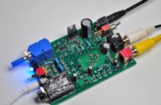 AmpCasqV3_Pluged_S.jpg148.7 KB · Views: 2,038
 -
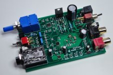 AmpCasqV3_Board_S.jpg161.6 KB · Views: 2,077
 -
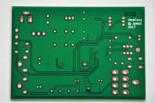 AmpCasqV3_PCB_B_S.jpg142.4 KB · Views: 2,060
 -
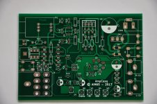 AmpCasqV3_PCBF_S.jpg168.3 KB · Views: 2,155
I dropped a huge clanger when I made a similar circuit.
I hadn't kept the power supply ground separate from the audio ground and got massive hum. I had randomly mixed in power supply ground with audio ground.
The power supply needs to be on its own on one corner/side of the pcb.
I hadn't kept the power supply ground separate from the audio ground and got massive hum. I had randomly mixed in power supply ground with audio ground.
The power supply needs to be on its own on one corner/side of the pcb.
Right, I had hum issues with the first version of pcb, then I spent some time on the ground plane and now it's dead silent.
Lm27761 is very sensitive to ground, I've spend a lot of time on it, now it as it's own ground plane on component side and it behave very well up to 200mA.
Lm27761 is very sensitive to ground, I've spend a lot of time on it, now it as it's own ground plane on component side and it behave very well up to 200mA.
Thanks for comments Sergey888.
To be honest I wasn't planning to do a high end headamp, only to go through all steps of project in order to have a finished and usable headmap, and also something I could share on DIYA.
Decoupling caps of OPA supply has been choosed to provide good value for price : nothing exceptional but Pana FR for ecap and Murata for the 100n MLCC Y7R 50V, 805 form factor. At 5V bias this cap is at 100% of its nominal value. Murata does publish the full specs of its capacitors on its website this is very useful. They’re located as close the chip as I could imagine being able to weld them…
I’v done some measurements with a scope with various load, they’re consistent with OPA1622 datasheet. It drive 32R paralled with 1nF up to 3.1Vp, while staying stable and it operating a cool temperature. Heatsink made in PCB is enough.
You’re right, so does nigelwright7557, layout is perfectible, I’ll keep that in mind for the next project !
Improving it does not mean that you need to spent tons of $$ on part - you just need to add and properly place a few fairly cheap components.
First of all 100nF caps have rather high impedance to really do a lot. It is necessary to provide a local low impedance path for at least high-ish audio frequencies. Something low-ESR around 220-470uF would be capable of doing it. And the reason for that not that much of a creeping signal products through a finite PSRR (also this is also can be a limiting factor) but inductive coupling supply rails, that caring highly distorted current, to signal lines. The longer those lines are - the more likely you'll get a trouble because of it. It is not the greatest idea to let them flow to the power supply.
The difference i'm talking about is not something you'll be able to see with a scope.
Have a look on some of my measurement results. On this level i managed to achieve something like 3-4dB improvement just by moving caps closer and keeping signals line further from supply.
http://www.diyaudio.com/forums/head...buffer-headamp-based-opa1622.html#post4703047
Could you elaborate a little on this, Nigel? E.g., do you mean that you kept these grounds completely separate? Or did they meet in a single spot? And, if so, did you connect them using a small inductor to keep out HF crud? Also, what would be the best place to have these grounds meet?I dropped a huge clanger when I made a similar circuit.
I hadn't kept the power supply ground separate from the audio ground and got massive hum. I had randomly mixed in power supply ground with audio ground.
The power supply needs to be on its own on one corner/side of the pcb.
BOM
Great,
I'll ship it tomorrow.
I've updated the BOM, there may be some slight differences with schematic.
BOM is for Farnell, I've put Farnell's references when available.
Attached is the BOM and the schematic in a more readable pdf format.
In addition, for the ones who plan to build AmpCasq and who never did solder smd before, I can send with the pcb a previous version of the pcb for training purposes.
Aim65,
PM sent and paypal for a board....thanks! Looking forward to building up this amp.
Thanks
Alex
Great,
I'll ship it tomorrow.
I've updated the BOM, there may be some slight differences with schematic.
BOM is for Farnell, I've put Farnell's references when available.
Attached is the BOM and the schematic in a more readable pdf format.
In addition, for the ones who plan to build AmpCasq and who never did solder smd before, I can send with the pcb a previous version of the pcb for training purposes.
Attachments
Nevermind....most of my existing wallworts will do!!
Alex
Yes, 10 V should be enough, it use 50mA idle and up to 100/150mA with a 50 Ohms headphone playing loud. So the main adapter should not be an issue, it should even work with an AC (non rectified) adapters, 12-14V mini
Pcb shipped
Board just shipped, delivery delay : 1 week
Aim65,
PM sent and paypal for a board....thanks! Looking forward to building up this amp.
Thanks
Alex
Board just shipped, delivery delay : 1 week
Great, now I have to figure out how to solder the really small parts, the 805's I have done on AGDR's ODA and other amps, but the smaller lead-less items will be a challenge to me. I have no hot air station etc...
Alex
It is doable. Since PCB has big vias in the thermal pads you can solder them with the strong soldering iron from the underside. The IC should align itself on the pad due to surface tension of the molten solder, but you can correct it carefully if it is slightly off to align the pins. Once thermal pad is done use the drag method on the pins by taking a lot of solder on the soldering iron tip. Apply a lot of flux and drag the tip along the package pins. Touch up if missed something. Remember to have a lot of solder on the tip otherwise it is nearly impossible to touch and heat the pins with the bare tip.
Hope it helps.
Oleg
Great, now I have to figure out how to solder the really small parts, the 805's I have done on AGDR's ODA and other amps, but the smaller lead-less items will be a challenge to me. I have no hot air station etc...
Alex
I use SMD tweezers to hold the part.
Rest your hand on the pcb holding the tweezers to keep your hand steady.
I solder one pad first then pick up part with tweezers and solder one pin to the tinned pad. I then solder the other pin.
- Status
- This old topic is closed. If you want to reopen this topic, contact a moderator using the "Report Post" button.
- Home
- Amplifiers
- Headphone Systems
- AmpCasq: an OPA1622 integrated headamp project