O2 headamp turn-on / turn-off thumps completely eliminated
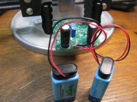
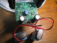
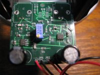
Well here some good news. I've figured out how to completely eliminate all turn-on / turn-off thumps with the O2 amplifer using the V3.0 booster board with the heaphone output relay.
The solution is shown in the pictures below:
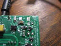
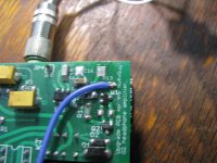
1. Unsolder the 100K R13 resistor from the V3.0 booster board. You won't need it anymore.
2. Cut a piece of 24 - 28AWG wire about 3.5 inches long (9cm). The wire just carries microamps so any gauge wire works here. Strip the ends back a couple of milimeters and tin the ends with solder.
3. Solder one end of the wire onto the R13 pad on the booster board that is closest to the edge of the board. The other R13 pad isn't used anymore.
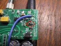
4. Solder the other end of the wire onto the end of R25 on the O2 PC board that is closest to the voltage regulators. From the photo you can see which one R25 is. Just put a small blob of solder on that end of the resistor first. Then heat it up and stick in the end of the wire.
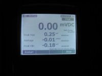
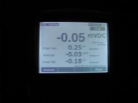
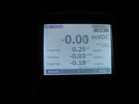
5. The three DMM shots are on the output of one channel, set for recording peak millivolt voltage levels. The first is with the O2 power switch off. The second is after the 8 second relay delay period, with the headphone relay on. You can see the 50uV DC offset measurement on the DMM on the top of the display. The final photo is with the O2 turned off. Absolutely zero turn-on and turn-off transients anymore.
And that is it! Enjoy your new completely thump-free O2 headamp + booster board combo.
Details:
From the above posts the turn-on thump is already gone with the new delayed turn-on headphone relay on the V3.0 board. The turn-off thump was reduced 90% as the peak meter readings showed. The turn-off thump is a tough one to eliminate entirely since it is caused by power rails collapsing. In the case of the O2 headamp that is further complicated by the power rails being turned on and off by the O2's power mosfets, which could happen for low battery as well as simply the power switch being turned off.
To get rid of turn-off thumps the relay circuit needs advance notice of the power switch being turned off, before any other circuitry "knows", to kill the relay. In the ODA headamp I did that by looping the relay coil through a spare set of contacts in the amp's on/off switch. No part of the amp has any further notice of a turn-off than the power switch, of course.
The O2 amplifier equivalent of the on/off switch is the gate circuit of the mosfets, fed by NwAvGuy's comparator circuit. The signals at the mosfet gates are the most advance notice of a turn off, either by the on/off switch or a low-battery mosfet cycle, in the O2 amp. The gate of the Q2 mosfet is turned off when the open collector output of the comparator goes to the negative rail, putting zero volts across the Q2 Vgs junction.
When the O2's comparator open-collector output turns off, the gate of Q2 is brought to the positive rail via R8 on the O2 PC board. Actually, it is brought up slowly by the R8-C21 RC combination. Once the gate of Q2 hits 2.1V or so it turns on.
What this modification is doing is essentially replacing the 100K R13 on the booster board (which returns to the positive rail after the mosfets) with a connection to the gate of Q2, and then using that same 270K R8 on the O2 PCB as a pull-up for Q1 on the booster board. So now when the O2's comparator open-collector goes low, to the negative rail, it not only shuts off Q2 on the O2 board but cuts power to the drain of Q1 on the booster board, which in turn turns off Q2 on the booster and cuts the relay power.
When the Q1 mosfet on the booster board turns on, during the 8 second relay turn-on delay period, it now shorts the gate to drain of Q2 on the O2 board. This has the effect of dropping the negative rail voltage by about 3v for those 8 seconds, but the relay and hence headphones are cut-off so it doesn't matter. Then the timing circuit finishes the 8 seconds, Q1 on the booster board turns off, the gate of Q2 on the O2 board is released, full negative rail returns, Q2 on the booster turns on and the relay turns on.
In the other direction, when the O2's comparator turns on the open collector output transistor and shorts the O2's Q2 gate to source, it also now cuts power to Q1 on the booster and immediately cuts off the relay, before the power rails have started to collapse.
Well here some good news. I've figured out how to completely eliminate all turn-on / turn-off thumps with the O2 amplifer using the V3.0 booster board with the heaphone output relay.
The solution is shown in the pictures below:
1. Unsolder the 100K R13 resistor from the V3.0 booster board. You won't need it anymore.
2. Cut a piece of 24 - 28AWG wire about 3.5 inches long (9cm). The wire just carries microamps so any gauge wire works here. Strip the ends back a couple of milimeters and tin the ends with solder.
3. Solder one end of the wire onto the R13 pad on the booster board that is closest to the edge of the board. The other R13 pad isn't used anymore.
4. Solder the other end of the wire onto the end of R25 on the O2 PC board that is closest to the voltage regulators. From the photo you can see which one R25 is. Just put a small blob of solder on that end of the resistor first. Then heat it up and stick in the end of the wire.
5. The three DMM shots are on the output of one channel, set for recording peak millivolt voltage levels. The first is with the O2 power switch off. The second is after the 8 second relay delay period, with the headphone relay on. You can see the 50uV DC offset measurement on the DMM on the top of the display. The final photo is with the O2 turned off. Absolutely zero turn-on and turn-off transients anymore.
And that is it! Enjoy your new completely thump-free O2 headamp + booster board combo.
Details:
From the above posts the turn-on thump is already gone with the new delayed turn-on headphone relay on the V3.0 board. The turn-off thump was reduced 90% as the peak meter readings showed. The turn-off thump is a tough one to eliminate entirely since it is caused by power rails collapsing. In the case of the O2 headamp that is further complicated by the power rails being turned on and off by the O2's power mosfets, which could happen for low battery as well as simply the power switch being turned off.
To get rid of turn-off thumps the relay circuit needs advance notice of the power switch being turned off, before any other circuitry "knows", to kill the relay. In the ODA headamp I did that by looping the relay coil through a spare set of contacts in the amp's on/off switch. No part of the amp has any further notice of a turn-off than the power switch, of course.
The O2 amplifier equivalent of the on/off switch is the gate circuit of the mosfets, fed by NwAvGuy's comparator circuit. The signals at the mosfet gates are the most advance notice of a turn off, either by the on/off switch or a low-battery mosfet cycle, in the O2 amp. The gate of the Q2 mosfet is turned off when the open collector output of the comparator goes to the negative rail, putting zero volts across the Q2 Vgs junction.
When the O2's comparator open-collector output turns off, the gate of Q2 is brought to the positive rail via R8 on the O2 PC board. Actually, it is brought up slowly by the R8-C21 RC combination. Once the gate of Q2 hits 2.1V or so it turns on.
What this modification is doing is essentially replacing the 100K R13 on the booster board (which returns to the positive rail after the mosfets) with a connection to the gate of Q2, and then using that same 270K R8 on the O2 PCB as a pull-up for Q1 on the booster board. So now when the O2's comparator open-collector goes low, to the negative rail, it not only shuts off Q2 on the O2 board but cuts power to the drain of Q1 on the booster board, which in turn turns off Q2 on the booster and cuts the relay power.
When the Q1 mosfet on the booster board turns on, during the 8 second relay turn-on delay period, it now shorts the gate to drain of Q2 on the O2 board. This has the effect of dropping the negative rail voltage by about 3v for those 8 seconds, but the relay and hence headphones are cut-off so it doesn't matter. Then the timing circuit finishes the 8 seconds, Q1 on the booster board turns off, the gate of Q2 on the O2 board is released, full negative rail returns, Q2 on the booster turns on and the relay turns on.
In the other direction, when the O2's comparator turns on the open collector output transistor and shorts the O2's Q2 gate to source, it also now cuts power to Q1 on the booster and immediately cuts off the relay, before the power rails have started to collapse.
Attachments
Last edited:
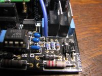
I forgot one step on the writeup above for the thump-less mod. Another one of the 10V zeners in the BOM (D2, the same type used across the relay coil) needs to be soldered into the "unused" R14 pad, with the banded end facing away from the edge of the PC board (toward R12). That R14 is listed as "do not populate" in the BOM. Now it gets populated. ")
The extra zener is to clamp the gate-source voltage of Q2 on the booster board to 10V, since that mosfet has a maximum Vgs of 20V. Without the zener the new modification would put 21 volts on that gate with fully charged batteries, 24V while on AC, and 30V with the +/-15Vdc O2 upgrade.
A gate voltage clamp is what R14 was originally used for when I posted that O2 modification a couple of years ago, part of a voltage divider with R13. That mod was intended to be used without a voltage regulator. After I sent the board to fab I realized that with the new 12V regulator R14 wasn't needed since the gate voltage wouldn't exceed 12V, but now with the new mod it is needed again. A zener is better than the resistive divider for the voltage clamp. The peak DMM milivolt readings I posted above showing no thumps were done with this new zener in place.
I will add all the information for the anti-thump modification to the V3.0 build instructions and BOM this weekend.
Also - unrelated - the 8 seconds I've been quoting for the turn-on time delay for the relay was from the math and Spice simulation, but I measured it today and is actually about 5 seconds. 5 seconds is better, 8 would have probably been a bit long. Keep in mind you can change that delay to just about anything by changing the values of C16 and C17.
Attachments
Last edited:
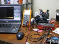
THD+N measurements
I just received a new toy, one of the Quant Asylum QA400 audio analyzers. Essentially just a USB soundcard in a box with dedicated software.
http://www.quantasylum.com/content/Products/QA400.aspx
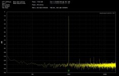
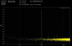
The plots below show the stock O2 on the left and the O2 + booster board on the right. I'm still getting familiar with the equipment so I may have a setting or test condition off here, but looks pretty good so far.
The O2 + O2 booster board seems to be matching or slightly beating the stock O2 THD + N within the margin of error, but adding the 93% output DC offset voltage reduction and zero-thump headphone relay.
I just received a new toy, one of the Quant Asylum QA400 audio analyzers. Essentially just a USB soundcard in a box with dedicated software.
http://www.quantasylum.com/content/Products/QA400.aspx
The plots below show the stock O2 on the left and the O2 + booster board on the right. I'm still getting familiar with the equipment so I may have a setting or test condition off here, but looks pretty good so far.
The O2 + O2 booster board seems to be matching or slightly beating the stock O2 THD + N within the margin of error, but adding the 93% output DC offset voltage reduction and zero-thump headphone relay.
Attachments
Last edited:
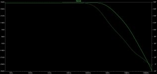
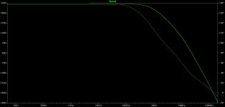
Limp - very, very good observation! There may be a longer story. 150 ohms is what NwAvGuy used in his frequency response measurements and plots on his website O2 page. I think there may be an O2 problem there.
While testing doing testing on the booster board I've subjectively noticed on the stock O2 (without the booster) slightly more bass, it seems, with the AC plugged in than with the batteries. Lack of bass has been something a lot of folks have posted about the O2 since it came out. Some have the problem, others seem to swear there is no problem. To try this, just start playing the O2 on AC on some song with a lot of bass and then pull out the AC plug. Then plug it back in. As long as the output swing is less than 5V rms or so (true for most headphones) running on AC or batteries should make no difference at all in the output voltage swing (volume).
Pondering the O2's circuit a bit as to why that would be the case, I noticed something. While on AC the O2 amplifier circuits are looking back into the output impedance of the LM7xxx voltage regulators which are nearly zero for frequencies under 1K, then only goes up an ohm or so to 20Khz.
But while on batteries, the amp circuit is looking back into the batteries. The voltage regulators are removed from the circuit by the diode logic. On a hunch I looked up the impedance characteristics of 9V batteries. For alkalines I've found a graph showing about 3 ohms at 100 ohms. That is huge IF the headphone are lower impedance, like most of mine. At 150 ohms, where NwAvGuy did his FR measurements, 3R (actually 6R round trip for both batteries) would hardly show up. So far I haven't found an impedance plot for "9V" NiMH, but I have seen postings indicating the impedence is worse for NiMH than alkaline, so it could even be higher than 3R at 100Hz.
Then I went back to NwAvGuy's frequency response postings on his blog, rather curious now at what impedance he measured things. And I was rather surprised when I saw it was 150 ohms. That is one of the big problems with a measurements-only amp design - a person might miss a certain measurement that matters, or in this case the test conditions on a measurement.
So I want to try quantifying that by re-running the O2 frequency response measurements with a 32 ohm load. In fact should be as easy as feeding in some low frequency signals and measuring the Vrms output with a sensitive DMM on AC, then again on batteries.
Now normally the 220uF bypass capacitors that NwAvGuy has across the power rails would solve the battery impedance problem. But... the impdenace of a 220uF capactor at 100Hz is about 7 ohms, worse than the battery it is bypassing, even though it is low ESR. It isn't big enough to properly bypass the low frequency signals around the batteries. Oddly enough NwAvGuy at one point posted "do not increase the value of this capacitor, it is already optimal" which itself sounds odd.
There would be a couple of possible O2 amp circuit fixes. The easy one is increasing the value of the two 220uF caps. Mouser has a 620uF that fits in the PCB space. I'm going to get those on order Tuesday. Those would drop the bypass impedance at low frequencies by 2/3. Another would be running the batteries through LDO voltage regulators, but that would be a major modification on another board.
Last edited:
Hi agdr
It is possible you reached the distortion limit of the analyzer. You can use a notch filter which may allow you to look deeper.
I completely agree! I'm actually in the process of whipping one up. I did a post on in the QA400 thread yesterday:
http://www.diyaudio.com/forums/equipment-tools/231401-quantasylum-qa400-17.html#post3821237
The noise floor that NwAvGuy came up with for the O2 headamp was more like -140dB, as I recall, using his dScope which he said had a max floor of -160dB. The loopback on the QA400 is around -130dB or so. I'm going to try a Fliege notch filter since it primarily uses resistors, which should make matching easier.
Notch Filter Calculator
I've found a 0.047uF 1% 50V COG/NPO MLCC for the single capacitor value. I originally had some rather huge 0.047uF 1% 650V polypropelene units in there, but COG should work nearly as well.
Today I've added a 50R pot to very slightly vary the center frequency around the 1kHz, taken from a TI filter app note on the Fliege here:
http://www.ti.com/lit/an/slyt235/slyt235.pdf (opens PDF)
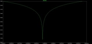
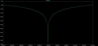
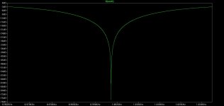
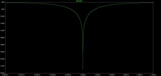
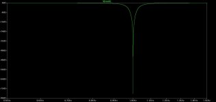
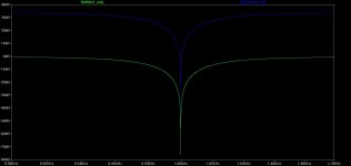
The range of the pot should be enough to compensate for the capacitor's 1%. In the QA400 thread a lot of folks have mentioned the importance of a defined bottom to the notch, like -20dB or -40dB, to know what, exactly, to subtract off the harmonics. That TI app note has a good suggestion. Don't use the bottom of the notch, but rather use the side of the well. In the plots below I've found that a 38Hz deviation from Fc will yeild -3dB, while a 4Hz deviation will give -20dB, if I'm looking at that right.
Interesting to note that the QA400 software has a built-in optional rounding function on the signal generator that causes the 1kHz signal to actually be generated at 1.002kHz on mine. From the 4Hz plot below that would automatically cause a -26dB deep notch without having to adjust a thing on the filter (assuming it was pre-nulled for whatever the capacitor's 1% variation causes).
Any suggestions are welcome! Those 10R power feed resistors on the op amps are actually your suggstion from the booster that I finally have the opportunity to try out. In fact I just realized I should give you credit on the board text for that.
I wouldn't have thought of that good idea for improving PSRR. I'm using 0805's here so I had enough board space to give it a try. The 10R + 1uF should put the corner frequency more-or-less where the PSRR on the LME49600 ramps up. Everything is at a notch filter Google Drive link now too:
https://drive.google.com/folderview?id=0B67cJELZW-i8ODk3VmNVOUc4MWM&usp=sharing
The LT Spice plots are for deviations from Fc of 500Hz, 100Hz, 38Hz (-3dB), 20Hz, and 4Hz (-20dB)
Attachments
-
 LT Spice ac plot 4Hz deviation.jpg34 KB · Views: 33
 -
 LT Spice ac plot 20Hz deviation.jpg33.4 KB · Views: 39
 -
 LT Spice ac plot 38Hz deviation -3dB.jpg38.7 KB · Views: 33
 -
 LT Spice ac plot 100Hz deviation.jpg30.8 KB · Views: 47
 -
 LT Spice ac plot 500Hz deviation.jpg26 KB · Views: 56
 -
 LT Spice circuit.jpg169.4 KB · Views: 80
 -
Fliege notch BOM 3.zip10.6 KB · Views: 37
-
 Fliege 1khz notch filter layout.png303.1 KB · Views: 86
 -
 Fliege 1khz notch filter circuit.png68.9 KB · Views: 78
Last edited:
Those 10R power feed resistors on the op amps are actually your suggstion from the booster that I finally have the opportunity to try out.
Because there is no class B output on the board driving low impedance load, unlikely you'll need this RC filtering. From other hand it will not hurt to put 0 Ohm links. Although I would try to ground decoupling capacitors trough a single via next to each opamp, and also move large caps closer to each other, to put their ground terminals as close as possible. It may help to avoid possible problems with return currents in the ground plane.
Makes sense to check if current noise of LME49990 will not dominate over other noise sources. If it is, beside lowering twin-T network impedance you may use an opamp with lower input current noise.
I'm being a bit paranoid, but it is also good practice to put positive and negative rails track in parallel to each other. This way total magnetic filed of those two tracks will contain more main signal harmonic than even harmonics. In case if you accidentally got a parasitic inductive coupling between the supply rails and a signal line, there will be a lower chance of picking up even harmonics. Again, it is more important when you have a class B/AB output stage driving a heavy load.
Sergey888 - thanks, all good suggestions. I did the ODA amp that way with parallel power traces for exactly the same reason, B field cancellation. I'll make that change. Also great idea about the single ground point for each op amp's decoupling caps. Yeah, I'm always a bit leery where return currents are flowing with solid ground planes. Under which parts and next to which parts.
Another interesting bit in that TI app note about the 100mHz THS op amp they used producing inadequate notch depth for a 100kHz notch - not enough bandwidth - but was adequate for a 10kHz notch. The LME49990 is 110mHz. I'm also using the same trick I did in the ODA and making good use of the chip's 600R drive capability. Smaller feedback resistors to lower the Johnson noise. Good point about the input current noise. I'll take a look at that and the trade-offs.
Another interesting bit in that TI app note about the 100mHz THS op amp they used producing inadequate notch depth for a 100kHz notch - not enough bandwidth - but was adequate for a 10kHz notch. The LME49990 is 110mHz. I'm also using the same trick I did in the ODA and making good use of the chip's 600R drive capability. Smaller feedback resistors to lower the Johnson noise. Good point about the input current noise. I'll take a look at that and the trade-offs.
Sergey888 - another idea. I've been wanting to build a notch filer + high gain amp pair to use as the input to the oscilloscope FFT. The new scope has a vertical sensitivity of 500uV/div, so a gain of 50x or so should do the job.
I'm thinking of stuffing an OPA637 in after the notch filter as the optional stage. The 637 is the uncompensated high-gain version of the OPA627 of course. As for compensation, I've used your 2nd order network. I've arranged the stage to be inverting, since current drive from the previous stage is no problem. I've added an optional zero ohm bypass around the 637 stage so that stuff can simply be left unpopulated, in which case the board reverts back to just a notch filter. As per your suggestion I've left the 10R's off that stage's power lines.
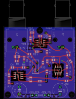
A lot of layout cleanup yet to do - may even put the parts on the board bottom - but here is a rough-in. Top layer is route, next is Vee, next is Vcc, and bottom is ground since the outer layer foil is twice as thick with Seeed's process.
I was able to get the ground on the C5 anc C6 decoupling on the same via. Wasn't able to share a via with C8 and C9 but at least I got them in the vicinity of each other. I'm still pondering the power routing.
I've been wanting to build a notch filer + high gain amp pair to use as the input to the oscilloscope FFT. The new scope has a vertical sensitivity of 500uV/div, so a gain of 50x or so should do the job. I'm thinking of stuffing an OPA637 in after the notch filter as the optional stage. The 637 is the uncompensated high-gain version of the OPA627 of course. As for compensation, I've used your 2nd order network. I've arranged the stage to be inverting, since current drive from the previous stage is no problem. I've added an optional zero ohm bypass around the 637 stage so that stuff can simply be left unpopulated, in which case the board reverts back to just a notch filter. As per your suggestion I've left the 10R's off that stage's power lines.
A lot of layout cleanup yet to do - may even put the parts on the board bottom - but here is a rough-in. Top layer is route, next is Vee, next is Vcc, and bottom is ground since the outer layer foil is twice as thick with Seeed's process.
I was able to get the ground on the C5 anc C6 decoupling on the same via. Wasn't able to share a via with C8 and C9 but at least I got them in the vicinity of each other. I'm still pondering the power routing.
Attachments
Last edited:
agdr
It is highly likely it will be unstable with a decompensated opamp like OPA637. In this case you can use something called phase lag-lead compensation, by placing series RC network in between inputs of the opamp. I'll find and example and post it later.
Also you may need a bandpass of low pass filter for you sig gen to get rid of harmonics.
Sergey888,
Sounds good, please do post any examples. I nearly tried some phase lead compensation - just a cap between the op amp inputs - while trying to wrap chips around the NJM4556A earlier in the thread.
Hey I've had an idea. Maybe the AD797 would be a good candiate for the high gain chip. I've stayed away from that chip since I've read a great many posts over the years from people trying to stop it from oscillating and eventually giving up. The chip apparently has a 110mHz GBP just like the LME49990, but the 49990 is unity gain stable. From one of the datasheet voltage follower diagrams it looks like the AD797 is unity gain stable, in a fashion, requiring matching resistances in the feedback loop and input. Probably not a good candiate for the Fliege filter op-amps since those circuits wind up at unity gain.
In the datasheet I see they consider the chip optimal for source resistances 1K or less, which would be the case for that inverting output stage. The data sheet also seems to like the inverting configuration for the chip. I recall having read something in the datasheet months ago about the chip's input bias current cancelling circuit needing some special care and feeding on the input, certain minimum input resistace, which is likely why that voltage follower configuration needs the resistances. I'll have to go back and read the whole datasheet again.
At any rate the AD797 would be cheaper, at $9.40, than the OPA637 at $25.
Attachments
Last edited:
Also you may need a bandpass of low pass filter for you sig gen to get rid of harmonics.
I forgot to say that I agree here, it certainly couldn't hurt from the AP photos that jackinnj posted of the QA400 output here, if I'm understanding that test correctly
http://www.diyaudio.com/forums/equipment-tools/231401-quantasylum-qa400-16.html#post3815567
A bandpass would help peel away the few remaining harmonics. If the filter is placed on the output of the generator it should be possible to use a purely passive bandpass, then just crank up the generator level to compesate for the filter insertion loss.
There is an example. It is pretty crude, but gives an idea. Don't pay attention to C1 - it is just a NE5534 model imperfection compensator
Basically you just manipulate a noise gain of the circuit on HF without affecting a signal gain. If you plot a loop gain of the circuit you'll see a section with 12dB/Oct roll off.
Basically you just manipulate a noise gain of the circuit on HF without affecting a signal gain. If you plot a loop gain of the circuit you'll see a section with 12dB/Oct roll off.
Attachments
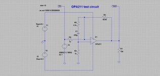
You can try OPA211 or OPA1611(2). They are quite linear and have reasonable current and voltage noise.
You were right.
The OPA211 looks like a good way to go after spending some time with that and the AD797 data sheets. Below is the lead-lag comp with the OPA211. I had been working with non-inverting circuits so long it wasn't until I graphed it and saw the phase that I realized a compensation capacitor from output to input isn't going to work with inverting. Pretty much would feed 180 degrees out of phase back to the input = oscillator.
What was I thinking. So I definitely see the need for the compensation on the input leads.470pf + your 2.1K seems to yeild a gain curve that is just slightly underdamped, flat through 50kHz with the 50x = 33dB voltage gain. The second plot is with 1000pF instead, a bit closer to critically damped.
The input circuit to the QA400 fries if fed more than 5V. I may add some clamp mechanism like running the input power through +/-5V regulators then to the op amps to limit their swing.
Attachments
Last edited:
Booster board also provides a 6x slew rate improvement
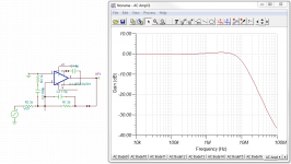
A recent set of postings about the O2 amp over on head-fi just made me realize the booster board provides another potential benefit: the slew rate is nearly 7 time faster than the O2's NJM4556A chips. The NJMs have a slew of 3V/uS, vs. 20V/uS for the OPA140. The LME49600's slew is something insane like 2000V/uS, but the OPA140's would be the limiting factor in the combination, of course.
The O2 amp's NJM2068 gain chip's slew is 6V/uS would would actually be the end-to-end limiting factor now. But... just pop in a LME49720 or pair of LME49990's on a dual SOIC8-to-dip adaptor and you now only get 20V/uS slew end to end, you get lower THD+N than the NJM2068 chip that also can make it through now due to the booster board chips.
NwAvGuy made a pretty good argument on his blog that no more than the NJM4556A's 3V/uS would ever be needed for headphone audio, given that is about the maximum present in any real-world recordings which limited by the signal processing chain. But there are some interesting arguments to the contrary out there. NwAvGuy's only negative comment about higher slew was opening up the potential for oscillation, which I have the scope shots to show isn't the case in this deisgn, at least out to 200mHz.
I'm experimenting with some SOIC8-to-dip adaptors for two LME49990 chips. If I can find one that fits properly in the U1 space on the O2, and can prove with the scope that it doesn't oscillate (or add bypassing as needed), I will probably make that the preferred gain chip upgrade to use with the booster board to take the O2 measurements to the next level.
Last edited:
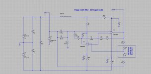
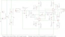
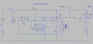
Fliege notch filter needs input R and current buffer
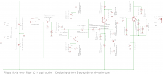
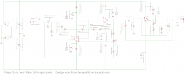
Here is some interesting info for anyone attempting the Fliege notch filter circuit posted above, in this case for the QA400 audio analyzer. I received my PCBs back yesterday and discovered a couple of things. Goes to show the importance of building and testing circuits! Stuff that looks good on paper can have some surprises in real life. I've never seen either of these issues mentioned about the Fliege notch filter circuit in all the Googling I've done to date.
First off it turns out some input resistance is required, otherwise the output will shoot down to the negative rail voltage when the input BNC is disconnected. I'm adding 10K across the input which results in about 1.2mV of DC offset. 100K results in about 16mV. Shorting the input, or hooking it to a headphone amp output with nearly zero impedance like the O2 or O2 booster board, results in just 600uV of output DC offset from the notch filter.
Since headphone amp outputs have the very low output impedence the problem doesn't show up when the Fliege notch filter input is connected to a headamp output. Also doesn't show up in the LT Spice sim since ideal voltage sources also have zero impedance. But when the filter input is disconnected on the PC board, or the filter input voltage source removed in Spice, the filter output zips down to a couple of volts above the negative rail, the maximum swing of the LME49990 chips if that input resistance is absent.
The reason is due to the capacitors in the Fliege filter being open circuits at DC (input signal removed from the filter). That effectively breaks one of the internal feedback loops and causes the op amps to act more like comparators. The polarity (negative rail) is due to the op amp inputs sourcing input bias current rather than sinking.
The other Fliege notch filter discovery is more serious. The LME49990 op amp doesn't have enough capacitive drive capability to power the 0.047uF cap in the middle of the Fliege filter circuit. The op amp is only rated for around 100pF of output drive capability before ringing effects start showing up. That would probabably be true for most of the 100mHz-or-so gain bandwidth op amps needed for the notch at 20kHz. The problem shows up as a distorted sine wave on the output of the Fliege notch filter, along with a modulation envolope effect at about a 250mS rate.
This particular problem is a little tricky to find in that it only shows up in the transient simulation of the notch filter. The notch vs. frequency in the AC simulation looks just fine either way. Also shows up on the scope looking at the filter output.
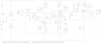
The solution is shown in the circuit below for a V2.0 of the Fleige notch filter. A BUF634 in the DIP8 package is now fed by the middle LME49990 op amp to provide adequate capacitive drive ability for that 0.047uF cap. The other solution would be to insert a small resistance (20 ohms does the trick) in series with the 0.047uF cap (after the op amp output) to isolatate the capacitance. Unfortunately that also affects the Q of the filter and shallows the notch. Using the current buffer chip preserves the notch depth, and the buffer is rated for the 110mHz GBP needed for the notch filter at 20kHz.
Some other improvements are using low noise TPS7A voltage regulators set for +/-5V to power everything. That way the maximum output level is limited to 5V, preventing the QA400 input (maximum 5 volts) from frying. The pre-amp stage is switched over to non-inverting so that a higher input impedance can be used while still keeping the feedback resistors small to limit Johnson noise. That high input impedence (10K) in turn allows a 4.7uF film coupling cap to be inserted at the input, blocking any DC offset coming from the Fliege notch filter stages and/or the headamp under test. Blocking the DC becomes especially important give that the stage voltage gain is 33dB (50x). A relatively small DC offset going into the pre-amp stage would result in a large DC output going into the QA400. It would also more or less negate the nice low 125uV input offset voltage of the OPA211 chip.
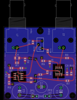
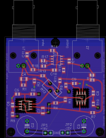
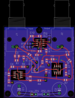
The BNC connectors are now mounted upside down on the bottom of the board to free up more top board space for parts, as is the new 4.7uF coupling cap. A switch is added for the incoming power. The incoming power filter caps are shrunk since they are no longer needed with the TPS7Axx voltage regulators and their low output impedance across the audio spectrum.
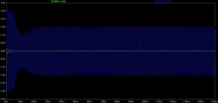
In the transient plot green is the output of the notch filter, about 33mV with a 200mV signal input at 1kHz, and the blue is the output of the 50x pre-amp fed by the notch filter. In actual practice using two of the Fliege notch boards in series would help drop the notch depth even further. The pre-amp circuit would be unpopulated on the first board.
Here is some interesting info for anyone attempting the Fliege notch filter circuit posted above, in this case for the QA400 audio analyzer. I received my PCBs back yesterday and discovered a couple of things. Goes to show the importance of building and testing circuits! Stuff that looks good on paper can have some surprises in real life. I've never seen either of these issues mentioned about the Fliege notch filter circuit in all the Googling I've done to date.
First off it turns out some input resistance is required, otherwise the output will shoot down to the negative rail voltage when the input BNC is disconnected. I'm adding 10K across the input which results in about 1.2mV of DC offset. 100K results in about 16mV. Shorting the input, or hooking it to a headphone amp output with nearly zero impedance like the O2 or O2 booster board, results in just 600uV of output DC offset from the notch filter.
Since headphone amp outputs have the very low output impedence the problem doesn't show up when the Fliege notch filter input is connected to a headamp output. Also doesn't show up in the LT Spice sim since ideal voltage sources also have zero impedance. But when the filter input is disconnected on the PC board, or the filter input voltage source removed in Spice, the filter output zips down to a couple of volts above the negative rail, the maximum swing of the LME49990 chips if that input resistance is absent.
The reason is due to the capacitors in the Fliege filter being open circuits at DC (input signal removed from the filter). That effectively breaks one of the internal feedback loops and causes the op amps to act more like comparators. The polarity (negative rail) is due to the op amp inputs sourcing input bias current rather than sinking.
The other Fliege notch filter discovery is more serious. The LME49990 op amp doesn't have enough capacitive drive capability to power the 0.047uF cap in the middle of the Fliege filter circuit. The op amp is only rated for around 100pF of output drive capability before ringing effects start showing up. That would probabably be true for most of the 100mHz-or-so gain bandwidth op amps needed for the notch at 20kHz. The problem shows up as a distorted sine wave on the output of the Fliege notch filter, along with a modulation envolope effect at about a 250mS rate.
This particular problem is a little tricky to find in that it only shows up in the transient simulation of the notch filter. The notch vs. frequency in the AC simulation looks just fine either way. Also shows up on the scope looking at the filter output.
The solution is shown in the circuit below for a V2.0 of the Fleige notch filter. A BUF634 in the DIP8 package is now fed by the middle LME49990 op amp to provide adequate capacitive drive ability for that 0.047uF cap. The other solution would be to insert a small resistance (20 ohms does the trick) in series with the 0.047uF cap (after the op amp output) to isolatate the capacitance. Unfortunately that also affects the Q of the filter and shallows the notch. Using the current buffer chip preserves the notch depth, and the buffer is rated for the 110mHz GBP needed for the notch filter at 20kHz.
Some other improvements are using low noise TPS7A voltage regulators set for +/-5V to power everything. That way the maximum output level is limited to 5V, preventing the QA400 input (maximum 5 volts) from frying. The pre-amp stage is switched over to non-inverting so that a higher input impedance can be used while still keeping the feedback resistors small to limit Johnson noise. That high input impedence (10K) in turn allows a 4.7uF film coupling cap to be inserted at the input, blocking any DC offset coming from the Fliege notch filter stages and/or the headamp under test. Blocking the DC becomes especially important give that the stage voltage gain is 33dB (50x). A relatively small DC offset going into the pre-amp stage would result in a large DC output going into the QA400. It would also more or less negate the nice low 125uV input offset voltage of the OPA211 chip.
The BNC connectors are now mounted upside down on the bottom of the board to free up more top board space for parts, as is the new 4.7uF coupling cap. A switch is added for the incoming power. The incoming power filter caps are shrunk since they are no longer needed with the TPS7Axx voltage regulators and their low output impedance across the audio spectrum.
In the transient plot green is the output of the notch filter, about 33mV with a 200mV signal input at 1kHz, and the blue is the output of the 50x pre-amp fed by the notch filter. In actual practice using two of the Fliege notch boards in series would help drop the notch depth even further. The pre-amp circuit would be unpopulated on the first board.
Attachments
Last edited:
- Home
- Amplifiers
- Headphone Systems
- O2 headamp output booster PCB