In my ongoing work to finish this project : http://www.diyaudio.com/forums/head...n-high-quality-class-lateral-fet-headamp.html I have made a few boards that will work in other projects as well.
It consists of a Power Switch Driver Board(PSDB) meant to be used in a powersupply and an Output Relay Board(ORB) meant to be used in a headphone amplifier. I designed both for use in a 2-box solutiuon with powersupply in one box and the headphone amplifier in another.
Details :
1. Power Switch Driver Board.
What it does : Enables the use of a Bulgin or similar anti-vandal momentary push-button.
One push of the button closes the mains rated relay and another opens the relay, making it easy to power on or off a transformer/powersupply.
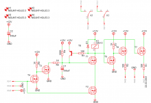
A simple design with a MAX6816 Debounce IC and a D flip-flop configured as a T(toggle) flip-flop which controls the relay.
Board needs a small separate transformer. Regulator for +12V(for relay, LEDs and output to ORB) as well as +5V(for the ICs) onboard.
It can also show the status of the board with 2 LEDs, one for ON and one for STANDBY.
Outputs +12V, GND and CTRL signal to ORB.
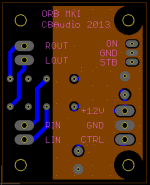
2. Output Relay Board.
What it does : Delays the output off the headphone amplifier when it is powered on for about 6-7 Sec before the output relay is activated, this delay is adjustable, on turn off the relay is opened immediately.
It is controlled by the CTRL signal from the PSDB. When the CTRL signal goes low and the relay is opened it takes about 2 sec before it can be turned on again with the full delay time available(C1 has to be discharged through R5, the discharge time could be lower depending on the exact values used for C1 and R5).
It can also show the status of the board with 2 LEDs, one for ON and one for STANDBY.
Needs +12V, GND and CTRL signal from PSDB to work.
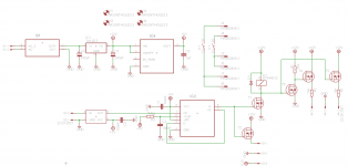
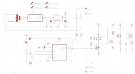
Attached is the schematics of both boards.
It consists of a Power Switch Driver Board(PSDB) meant to be used in a powersupply and an Output Relay Board(ORB) meant to be used in a headphone amplifier. I designed both for use in a 2-box solutiuon with powersupply in one box and the headphone amplifier in another.
Details :
1. Power Switch Driver Board.
What it does : Enables the use of a Bulgin or similar anti-vandal momentary push-button.
One push of the button closes the mains rated relay and another opens the relay, making it easy to power on or off a transformer/powersupply.
A simple design with a MAX6816 Debounce IC and a D flip-flop configured as a T(toggle) flip-flop which controls the relay.
Board needs a small separate transformer. Regulator for +12V(for relay, LEDs and output to ORB) as well as +5V(for the ICs) onboard.
It can also show the status of the board with 2 LEDs, one for ON and one for STANDBY.
Outputs +12V, GND and CTRL signal to ORB.
2. Output Relay Board.
What it does : Delays the output off the headphone amplifier when it is powered on for about 6-7 Sec before the output relay is activated, this delay is adjustable, on turn off the relay is opened immediately.
It is controlled by the CTRL signal from the PSDB. When the CTRL signal goes low and the relay is opened it takes about 2 sec before it can be turned on again with the full delay time available(C1 has to be discharged through R5, the discharge time could be lower depending on the exact values used for C1 and R5).
It can also show the status of the board with 2 LEDs, one for ON and one for STANDBY.
Needs +12V, GND and CTRL signal from PSDB to work.
Attached is the schematics of both boards.
Attachments
Last edited:
Design of both is done.
No changes to the Output Relay Board Schematic.
The Power Switch Driver Board has been redesigned and simplified compared to what I started out with.
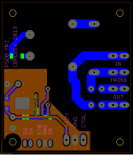
Attached is PSDB Schematic, PSDB Layout, ORB Layout.
There is 3mm between live and neutral and a minimum of 10mm between mains voltage and secondary low voltage circuits as well as the PCB stand offs.
No changes to the Output Relay Board Schematic.
The Power Switch Driver Board has been redesigned and simplified compared to what I started out with.
Attached is PSDB Schematic, PSDB Layout, ORB Layout.
There is 3mm between live and neutral and a minimum of 10mm between mains voltage and secondary low voltage circuits as well as the PCB stand offs.
Attachments
Last edited:
- Status
- This old topic is closed. If you want to reopen this topic, contact a moderator using the "Report Post" button.