Improved DC Servo for O2 amp output stage
I've posted a schematic and discussion for a high accuracy DC servo for the output stage of Rocket Scientist's O2 headphone amp here as a wiki page:
DC Servo For O2 Headphone Amp Output Stage - diyAudio
Figured that I would give the site's wiki system a try.") The circuit is based on a fixed/upgraded version of the DC servo in the National Semiconductor LME49600 evaluation board. The circuit uses a OPA627 for high DC accuracy for input offset voltage and extremely low input bias current (FET input). The circuit makes use of a 3 pole passive input low pass filter to extract DC from the O2's output signal with just 40uV of AC ripple left on it, about half the maximum input offset voltage of the OPA627, effectively pure DC for purposes here.
The circuit is based on a fixed/upgraded version of the DC servo in the National Semiconductor LME49600 evaluation board. The circuit uses a OPA627 for high DC accuracy for input offset voltage and extremely low input bias current (FET input). The circuit makes use of a 3 pole passive input low pass filter to extract DC from the O2's output signal with just 40uV of AC ripple left on it, about half the maximum input offset voltage of the OPA627, effectively pure DC for purposes here.
The goal of this servo is to zero out the 3mV or so of DC offset voltage on the O2 amps outputs caused by the 1.5mV or so input offset voltage of the NJM4556 chips, plus their relatively high input bias current pulled through the 40.2K resistors to ground causing an additional IR drop that is added to the NJM4556 input. The servo allows those resistors to be bumped up to 160k, reducing the low frequency cutoff of the output stage coupling cap filter. The caps can also be increased to 4.7uF, as mentioned in one of the mods above, for even a lower Fc.
The servo likely won't make any audible difference, and as per AKG tech support really won't even matter for most phones since a 3mV deviation of the diaphram out of 130mV or so of excursion range really doesn't matter. However many folks like the idea of the transducers in the headphones sitting at their natural resting positions, not 3mV one way or the other. The small 3mV offset might make a difference in some sensitive IEMs.
I've posted a schematic and discussion for a high accuracy DC servo for the output stage of Rocket Scientist's O2 headphone amp here as a wiki page:
DC Servo For O2 Headphone Amp Output Stage - diyAudio
Figured that I would give the site's wiki system a try.
The circuit is based on a fixed/upgraded version of the DC servo in the National Semiconductor LME49600 evaluation board. The circuit uses a OPA627 for high DC accuracy for input offset voltage and extremely low input bias current (FET input). The circuit makes use of a 3 pole passive input low pass filter to extract DC from the O2's output signal with just 40uV of AC ripple left on it, about half the maximum input offset voltage of the OPA627, effectively pure DC for purposes here.The goal of this servo is to zero out the 3mV or so of DC offset voltage on the O2 amps outputs caused by the 1.5mV or so input offset voltage of the NJM4556 chips, plus their relatively high input bias current pulled through the 40.2K resistors to ground causing an additional IR drop that is added to the NJM4556 input. The servo allows those resistors to be bumped up to 160k, reducing the low frequency cutoff of the output stage coupling cap filter. The caps can also be increased to 4.7uF, as mentioned in one of the mods above, for even a lower Fc.
The servo likely won't make any audible difference, and as per AKG tech support really won't even matter for most phones since a 3mV deviation of the diaphram out of 130mV or so of excursion range really doesn't matter. However many folks like the idea of the transducers in the headphones sitting at their natural resting positions, not 3mV one way or the other. The small 3mV offset might make a difference in some sensitive IEMs.
How/were to solder .01 to .1 uF bypass caps. in O2
Pls read "A question about bypass cap." #3092 & comments by sofspud & gootee on page 310.
http://www.diyaudio.com/forums/head...ective2-o2-headphone-amp-diy-project-310.html
Since you are good at hacking /moding O2(& many more things) at the same time having measuring instruments to chk. your hacks/mods can you pls test if bypass caps(.01 to .1 uF) at U1 and maybe at U2/U3 can change the performance of O2 w.r.t. transient response or HF stability.
Pls read "A question about bypass cap." #3092 & comments by sofspud & gootee on page 310.
In the case of the O2, my two cents is you are OK with what RocketScientist has in place for bypassing. The speed of the chips involved and the speed of the information going through figure into things, since the problem is inductance in the traces. The NJM2068 and NJM4556A are both "audio" chips that just are not all that fast, which is fine (preferable) for audio and less likely to launch into HF oscillations.
By way of comparison, take a look at what OPC has done in the "Wire" for bypassing (schematic link at the bottom):
"The Wire" Headphone Amp Build Wiki - diyAudio
Now there the LME49600 is another animal entirely. That is a "video" chip that is fast enough to pass video and does require what you are saying. OPC has 10uF X7R MLCC ceramics right at the pins of the LME49600, which is a great design imho. In the LME49600 evaluation board data sheet they have 1uF X7Rs in parallel with 10uF tantalums at each rail to ground, as I recall, but those were likely the days before you could just buy a 10uF X7R MLCC. A ceramic cap is good at high(er) frequencies. The 10uf is for energy storage while the MLCC ceramic is to nuke HF oscillations. The one 10uF XLR MLCC gives you both.
Same holds for the LME49990. The gain-bandwidth product on that guy is 110mHz! Compared to a GBW of just 19mHz for the NJM2068. Again OPC has put 1uF X7R MLCCs right at the pins. Less energy storage is needed with the gain chip than with the high current output chip there, hence the lower capacitance for the bypass cap.
Like sofaspud posted in #3094 I had one 10uF MLCC X7R sitting between the two OPA627 chips in the ODA layout I posted yesterday in an earlier layaout where the chips were further away from the power supply caps. In that case I just had one cap going rail to rail, none rail to ground. The power lines fed the cap which then star'ed off to the chips on either side. I may add it back, actually, was thinking about that today.
Bypassing can get into a real religious discussion!
Lots of good thoughts on it all out there.
Last edited:
In the case of the O2, my two cents is you are OK with what RocketScientist has in place for bypassing.....
That cleared my doubts.BTW I'm atheist
agdr, I'm looking at your Bass-boost mod.
I'm curious as to how one would bring the frequency + bandwidth down, I'm hoping to achieve +10dB at 30hz and about +5dB at 60Hz and maybe about +1dB(or less) at 100hz
I'm really in to my Subbass and considering my Headphones naturally drop to -10dB at 20hz.
I was originally looking at doing this Passive RC low-shelf pass but your method looks more interesting.
I'm hoping to achieve +10dB at 30hz and about +5dB at 60Hz and maybe about +1dB(or less) at 100hz
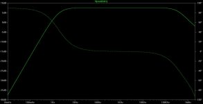
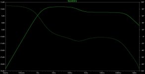
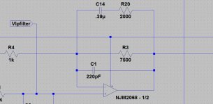
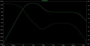
The first order filter in the boost circuit can't roll off quite that fast, but can get in the ballpark. Looks like the closest it can get is with the values below, 0.39uF and 2K for the boost part and 7.5K for the regular feedback resistor. The circuit winds up looking a lot like the rightmost diagram in your link for the shelving filters, except their configuration is for an inverting op amp and here it is non-inverting.
In the plots below the first is an O2 with no bass boost. The second is the regular boost parts, and the 3rd is with these values. The net result is:
10Hz 18dB (+10.3dB)
30Hz 16.7dB (+9dB)
60Hz 14.3dB (+6.6dB)
100Hz 11.5dB (+3.8dB)
273Hz 8.7dB (+1dB)
from 1Khz on 7.7dB.
If you need less than 7.7dB of gain (2.5x) after 1kHz use the attenuation mod earlier in this thread to knock the incoming signal down as needed. That modification just substitutes a larger value for the incoming 274R resistor to form a voltage divider with the 10k resistor to ground on the input of the O2. For example, if the 274R is replaced with a 10K that would form a 50/50 voltage divider. The input signal would get cut in half, then 2.5x from 1Khz on, yielding about 1.25x. The boost amount would get cut in half though, too, with the attenuation mod. In that case the amount of boost would need to be doubled to compensate.
Attachments
Last edited:
Thanks! I have LTSpice open with the Passive RC design in it and it looks like it suffers from the same bandwidth issues, my current one is peaking around 4hz , and hitting (-9.5dB) at 100hz.
The only way I can see getting it to work my way is to peak it near 1hz at +20dB, so the slope lands at +10dB at 20Hz, and 1dB at 100hz. I would never consider this except the other shelf filter has a -8dB from peak at 1hz which might offset this excessive gain.
The only way I can see getting it to work my way is to peak it near 1hz at +20dB, so the slope lands at +10dB at 20Hz, and 1dB at 100hz. I would never consider this except the other shelf filter has a -8dB from peak at 1hz which might offset this excessive gain.
The only way I can see getting it to work my way is to peak it near 1hz at +20dB, so the slope lands at +10dB at 20Hz, and 1dB at 100hz.
Yes, that might do the job! Certainly worth trying. I messed around with that a bit, trying for just the last half or so of the roll-off curve, but it never seemed like the roll-off was steep enough to hit the 30Hz, 60Hz, and 100Hz specs. My guess is at least a second order filter would be needed in the feedback loop to get a steeper slope. I don't see a way to do that offhand with the shelving effect. A 2nd order MFB or salen key wouldn't level off, they would just keep going. Maybe someone out there has worked this out before and will post.
Seems like the kind of thing that would come up a lot with subwoofers.A LME49720HA on an adapter fits in for the NJM2068 gain chip
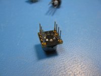
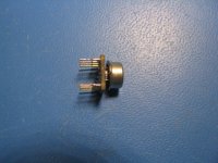
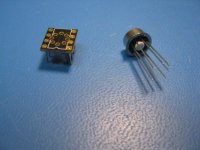
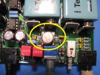
I just discovered that a metal can LME49720HA chip on a Brown Dog #02601B TO99 - to - DIP8 adaptor fits in just fine for the NJM2068 gain chip in the O2 headamp. Sounds pretty good too! No oscillations at all out to the 55MHz GBP of the chip and the 200MHz bandwidth of the scope.
The adaptor is this one. The leads on the chip have to be trimmed before inserting it in the adaptor. Then it takes some fairly precision soldering with a fine tip and small gauge solder to go around the circle - not recommended for first time solderers.
Attachments
Last edited:
I found some adapters on another forum that don't even require soldering it simply just slides onto the pins and spreads them out to fit a dip socket. This isn't my pic but it's the white plastic thingie
[URL=http://s1277.photobucket.com/user/fsatsil/media/1eabe860b0301d0bd82af67f16ec78a0_zps1ae716ef.jpg.html]
[URL=http://s1277.photobucket.com/user/fsatsil/media/1eabe860b0301d0bd82af67f16ec78a0_zps1ae716ef.jpg.html]
An externally hosted image should be here but it was not working when we last tested it.
[/URL]I found some adapters on another forum that don't even require soldering it simply just slides onto the pins and spreads them out to fit a dip socket.
Hey nice find! I didn't know about those. I noticed those leads on the LME49720HAs were extremely long. I'll bet T.I. had this in mind.
Throwing away some open loop gain for better (subjective!) sound & 5K pot mod
This modification is something to try for those folks using gains greater than 1 in their O2 headamps. This one is a subjective O2 modification, which of course runs counter to NwAvGuy's 100% objective "if it measures well it sounds the best" philosophy, but I'm only 50% on the objective thing myself.
I've seen a number of posts since NwAvGuy released the O2 headamp that essentially say "my O2 sounds better on the high gain 2.5x position with the volume control turned down than on the low gain 1x position with the volume control up". They promptly get shot down since that can't possibly be the case, right?
I've kind of noticed the phenomenon myself and recently ran into this interesting post from Nelson Pass a decade ago. He is essentially saying that from subjective listening experiences, an op amp at unity gain or low closed-loop gain may be so close to oscillation that it affects the sound. His solution is to throw away some of the open loop gain.
To try this with the gain stage in the O2 headamp with an overall 2x voltage gain, do this:
1. Set the low (closed loop) gain switch position to be 6.5x with R17=R21=274R, the highest that NwAvGuy recommends with the (compensated) NJM2068 op amp. This will come in well under Nelson's 20dB recommendation in that post. To go higher consider replacing the NJM2068 with a dual LME49990 on an adaptor. The NJM2068 open loop gain is listed as 90dB minimum, whereas the LME49990 is 120dB minimum. With the LME49990 try setting the gain to be 12x with R17=R21=137R.
2a. If using the NJM2068 with a 6.5x closed loop gain, replace the R14=R20 ground return resistors with 1.5K (from 10K in the BOM), the series RF filter resistors R3=R7 with 4.99K (from 274R in the BOM), and the RF filter capacitors C11=C12 with 12pF (from 220pF) in the BOM. The 4.99K resistor forms a voltage divider with the 1.5K resistor to knock the signal down by 70%. When applied to the 6.5x gain setting the net result will be a 2x signal gain. The capacitor change just keeps the RF filter corner frequency around NwAvGuy's original 2.6mHz.
2b. If using a dual LMe49990 with 12x closed loop gain, replace the R14=R20 ground return resistors with 1.5K (from 10K in the BOM), the series RF filter resistors R3=R7 with 9.1K (from 274R in the BOM), and the RF filter capacitors C11=C12 with 8pF (from 220pF) in the BOM. The 9.1K resistor forms a voltage divider with the 1.5K resistor to knock the signal down by 85%. When applied to the 12x gain setting the net result will be a 2x signal gain. The capacitor change just keeps the RF filter corner frequency around NwAvGuy's original 2.6mHz.
A handy by-product of the change with either gain chip is lowering the impedance looking out the non-inverting input to be a closer to match to that looking out the inverting input (the feedback network, which is all low-ohm resistors).
One downside is that these changes will result in more noise, both from the higher Johnson noise from the larger input series resistor and then the gain stage amplifying that noise with the 6.5x/12x voltage gain. But the level will still likely be below hearing thresholds.
If you are using the dual LME49990 adaptor option you can make another modification to further lower that noise. The LME49990 is THD+N rated down to a 600R load in the datasheet vs. just 2K load for the NJM2068. So the O2's volume control can be reduced to 5K (from 10K in the O2 BOM), the output stage ground return resistors changed to 24.9K (from 40.2K in the BOM), and the coupling capacitors to 4.7uF with Mouser part number #505-MKS2-4.7/50/10 (which are the same physical size as the 2.2uF caps in the BOM). The change in volume control and coupling caps lowers the corner frequency on the low end of the O2's frequency response curve to 1.37hz from 1.8Hz.
Reducing the values of the volume control and ground return resistors like this will lower the Johnson noise vs. the O2 BOM values and recover some of the (lower) noise floor. The total load on the gain chip will be the pot in parallel with the 1.5K feedback network, or around 1.15K vs. the chip 600R miminum. Another side benefit of the 5K pot vs. the BOM 10K is potentially lower input impedance distortion from the output stage at mid volume control. Looking back into the 5K pot at mid-setting gives just 1.25K vs. 2.5K for the 10K pot.
Note on a possible point of confusion on those coupling capacitors! The 4.7uF's are the 50Vdc/30Vac units while the O2 BOM 2.2uF's are the 63Vdc/40Vac caps. Page 35 in the datasheet at first quick read makes it seem like the 40Vac units would have thermal problems with a 7Vrms swing at 20kHz. But that table only applies to situations where the full ripple voltage is across the capacitor, such as bypass and power filter duty. For coupling usage the voltage across the capacitor is nearly zero through the audio band, resulting in 80kHz or greater limits from that chart.
Last edited:
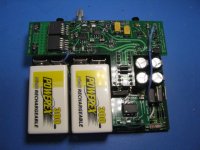
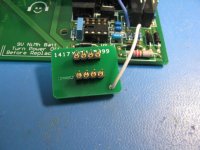
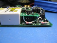
O2 non-motorboat PM latch board and post 108 update
I have an update to post #108 above from way back when that has my latch circuit for NwAvGuy's power management circuit in his O2 headphone amplifier.
The sense wire that goes to the O2's mosfets needs to go to the other end of the O2's R24. In post 108 I show that connection going to the side of the O2's R24 that is the Q1 mosfet gate, but it should go to the other comparator side of R24. On the O2 PC board that is the end of R24 closest to the O2's voltage regulators. I have photos posted below of the V1.0 board which shows how it wires into the O2.
Another update is the 4.7 meg resistor in post #108 should be around 499K instead. With 499K the O2 only has to be turned off (with the O2 power switch) for 10 seconds to reset the latch circuit. With the previous 4.7 meg it was more like 40 seconds, which was annoying.
Details, for those interested:
That circuit in post #108 solves the problem of the O2 headphone amp producing a "motorboating" sound at 2Hz or so when the batteries run down and the O2's power management circuit tries to shut them off. All batteries rise up in voltage a bit when the load is cut off. If that rise is too much with the O2's 9V NiMH batteries the PM circuit is fooled into thinking the batteries are charged again and turns the amp back on. With the load restored the voltage drops and the PM circuit shuts it all off again. It just sits there and does that over and over at 2 times per second or so, producing that motorboat sound in the headphones.
The circuit has worked fine since I posted it two years ago except for one thing. If the O2 is running on batteries plugging the AC power adaptor in would trigger the latch circuit. The O2 power switch would have to be turned off each time for the 10 seconds to reset the latch circuit. Moving the sense wire to the other side of the O2's R24 solves the problem. The latch won't trigger now if the AC power is plugged in.
The "why" the problem occured is pretty tricky. NwAvGuy has 0.022uf capacitors on the gate of each O2 mosfet to act as a turn-on delay in an effort to prevent turn-on thumps. Those 0.022uF caps charge up to the full rail-to-rail voltage when the O2's mosfets are on. In the case of batteries that would be a minimum of 14Vdc or a maximum of around 20Vdc.
When the O2's power supply rails suddently shoot up to 24Vdc with the AC adaptor plugged in those fully-charged 0.022uF caps act like small batteries for a few milliseconds, such that the gate voltage goes from being zero with respext to the negative rail to 24V - the capacitor voltage. If the batteries were at 20V rail to rail that would be 24Vdc - 20Vdc = 4Vdc, which is more than enough to turn on the top mosfet in the latch circuit's two mosfet stack and trigger the latch. If the batteries are at the discharge end of 14Vdc rail to rail that voltage is even worse at 14Vdc.
But the other end of the O2's R24 is connected to the comparator's open collector transistor output, which is on and clamped to negative rail. So regardess of the 0.022uF cap acting like a mini battery the other end of R24 will stay firmly at 0 volts with respect to the negative rail and won't falsely trigger the latch circuit.
Lol - only took me 2.5 years to figure that out!
With that problem resolved I've just reworked the board to be smaller, using a SOIC-8 version of the O2's NJM2903d (or LM2903) and 0805 sized resistor and capacitor. The V 1.0 board is large enough that I've been using a drop of hot glue on the side of the O2's U2 IC socket and the pluggable header to make sure the board stayed in the socket. The V2.0 board shouldn't need that.
The schematic, layout, BOM, build instructions, etc. are here on Google Drive:
https://drive.google.com/folderview...NvRjBCNU9BTmpMazcwLWY2VnNkdVdjdzg&usp=sharing
The V 2.0 folder is the one that just went out for fab. If it tests OK when back I'll post the Gerber files. I'm not going to bother posting the same stuff for the V 1.0 board that has been around for a year since its being replaced, other than the V1.0 folder has the photos below showing where that sense wire solders to on the O2 PC board.
I have an update to post #108 above from way back when that has my latch circuit for NwAvGuy's power management circuit in his O2 headphone amplifier.
The sense wire that goes to the O2's mosfets needs to go to the other end of the O2's R24. In post 108 I show that connection going to the side of the O2's R24 that is the Q1 mosfet gate, but it should go to the other comparator side of R24. On the O2 PC board that is the end of R24 closest to the O2's voltage regulators. I have photos posted below of the V1.0 board which shows how it wires into the O2.
Another update is the 4.7 meg resistor in post #108 should be around 499K instead. With 499K the O2 only has to be turned off (with the O2 power switch) for 10 seconds to reset the latch circuit. With the previous 4.7 meg it was more like 40 seconds, which was annoying.
Details, for those interested:
That circuit in post #108 solves the problem of the O2 headphone amp producing a "motorboating" sound at 2Hz or so when the batteries run down and the O2's power management circuit tries to shut them off. All batteries rise up in voltage a bit when the load is cut off. If that rise is too much with the O2's 9V NiMH batteries the PM circuit is fooled into thinking the batteries are charged again and turns the amp back on. With the load restored the voltage drops and the PM circuit shuts it all off again. It just sits there and does that over and over at 2 times per second or so, producing that motorboat sound in the headphones.
The circuit has worked fine since I posted it two years ago except for one thing. If the O2 is running on batteries plugging the AC power adaptor in would trigger the latch circuit. The O2 power switch would have to be turned off each time for the 10 seconds to reset the latch circuit. Moving the sense wire to the other side of the O2's R24 solves the problem. The latch won't trigger now if the AC power is plugged in.
The "why" the problem occured is pretty tricky.
NwAvGuy has 0.022uf capacitors on the gate of each O2 mosfet to act as a turn-on delay in an effort to prevent turn-on thumps. Those 0.022uF caps charge up to the full rail-to-rail voltage when the O2's mosfets are on. In the case of batteries that would be a minimum of 14Vdc or a maximum of around 20Vdc. When the O2's power supply rails suddently shoot up to 24Vdc with the AC adaptor plugged in those fully-charged 0.022uF caps act like small batteries for a few milliseconds, such that the gate voltage goes from being zero with respext to the negative rail to 24V - the capacitor voltage. If the batteries were at 20V rail to rail that would be 24Vdc - 20Vdc = 4Vdc, which is more than enough to turn on the top mosfet in the latch circuit's two mosfet stack and trigger the latch. If the batteries are at the discharge end of 14Vdc rail to rail that voltage is even worse at 14Vdc.
But the other end of the O2's R24 is connected to the comparator's open collector transistor output, which is on and clamped to negative rail. So regardess of the 0.022uF cap acting like a mini battery the other end of R24 will stay firmly at 0 volts with respect to the negative rail and won't falsely trigger the latch circuit.
Lol - only took me 2.5 years to figure that out!
With that problem resolved I've just reworked the board to be smaller, using a SOIC-8 version of the O2's NJM2903d (or LM2903) and 0805 sized resistor and capacitor. The V 1.0 board is large enough that I've been using a drop of hot glue on the side of the O2's U2 IC socket and the pluggable header to make sure the board stayed in the socket. The V2.0 board shouldn't need that.
The schematic, layout, BOM, build instructions, etc. are here on Google Drive:
https://drive.google.com/folderview...NvRjBCNU9BTmpMazcwLWY2VnNkdVdjdzg&usp=sharing
The V 2.0 folder is the one that just went out for fab. If it tests OK when back I'll post the Gerber files. I'm not going to bother posting the same stuff for the V 1.0 board that has been around for a year since its being replaced, other than the V1.0 folder has the photos below showing where that sense wire solders to on the O2 PC board.
Attachments
Last edited:
Anybody have a limiter circuit to share for the O2?
I haven't seen anybody publish one. With the O2's design of the pot after the gain stage it is entirely possible to overload the gain stage and send it into clipping, before the signal even reaches the pot, without being aware of it. I "solved" that problem with my O2 Desktop Amp design by adding a clipping indicator LED to at least give people a visual indication of clipping. I used a window comparator to drive the LED.
An actual limiter, especially for peaks, would certainly be another way to do it.
FWIW, I nagged NwAvGuy a bit back in the day via PM and email about adding a clipping indicator circuit after the O2 was released. At the time I just couldn't fathom not having some indication of clipping on a gain stage with variable gain that didn't have a pot in front. But his view was that clipping was unlikely given typical audio source levels and typical gains. Plus the O2's PC board was out of space to add any additional circuitry and he wanted to stay all through-hole.
Last edited:
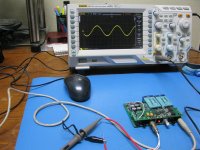
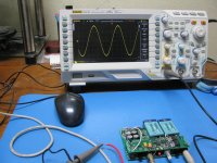
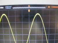
Scope photos for the 1/3 input attenuation modification + RF cap change
I just installed the 1/3 input attenuation modification in post #12 in an O2 and had an opportunity to take some scope shots of the results.
Post #12 has the details, but in a nutshell the O2's 274 ohm input resistors, which are part of the RF filter with a 220pF capacitor, is replaced with a 4.99K resistor to form a 1/3 - 2/3 voltage divider with the O2's 10K pot. The net result is a 1/3 attenuation of the input signal (2/3 signal pass-through) to help deal with "hot" (high level) input sources.
All the O2's gain settings then get multiplied by the new 2/3 pass-through. If you had the standard 1x / 2.5x gain settings before, you wind up with 0.67x / 1.7x. If you wish to maintain 2.5x for the higher gain setting just bump the gain up in that setting so the product with 0.67 equals 2.5, a 549 ohm "gain" resistor in this case, Mouser #270-549-RC or #71-CMF50549R00FHEB.
The RF filter capacitor is correspondingly reduced to maintain the corner frequency from the previous filter. However here is one change over what I wrote in post #12. NwAvGuy had the corner frequency set at 2.6mHz. In post #12 I saw fit to reduce that to 470kHz. If you want to stay closer to NwAvGuy's original corner the cap to use would be a 12pF, a Mouser #80-C315C120K5G (Kemet #C315C120K5G5TA, 50V COG MLCC 2.54mm lead spacing).
The O2 being used here has gain set at 1x and 5.1x before the attenuation. After the attenuation these should be [(1 * 0.67) = 0.67x] and [(5.1 * 0.67) = 3.4x]. The O2 has an O2 Booster Board installed, but the Booster Board has 1x voltage gain, just a current buffer. Lets see if the measurements match up...
Photos with the modification in place:
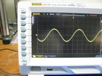
* The first two show the test setup and input signal, 1V peak (2Vp-p) at 1kHz. The scope is on 500mV/division, which shows up in the lower left corner of the screen.
* In the next 2 photos show the O2 on the low gain setting (gain button out), 1Vpeak input, volume control all the way up. The scope is still on 500mVdiv so the small ticks in-between divisions are 100mV. As the close-up in 4453 shows, 0.67V peak! Right on the money.
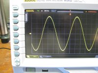
* The next 3 show the O2 on high gain, gain button pushed in. The scope is now on 1V/div with the minor ticks now at 200mV. The close-up in 4460 shows 3 major divisions and 2 minor, which would be 3.4Vpeak, as expected.
I just installed the 1/3 input attenuation modification in post #12 in an O2 and had an opportunity to take some scope shots of the results.
Post #12 has the details, but in a nutshell the O2's 274 ohm input resistors, which are part of the RF filter with a 220pF capacitor, is replaced with a 4.99K resistor to form a 1/3 - 2/3 voltage divider with the O2's 10K pot. The net result is a 1/3 attenuation of the input signal (2/3 signal pass-through) to help deal with "hot" (high level) input sources.
All the O2's gain settings then get multiplied by the new 2/3 pass-through. If you had the standard 1x / 2.5x gain settings before, you wind up with 0.67x / 1.7x. If you wish to maintain 2.5x for the higher gain setting just bump the gain up in that setting so the product with 0.67 equals 2.5, a 549 ohm "gain" resistor in this case, Mouser #270-549-RC or #71-CMF50549R00FHEB.
The RF filter capacitor is correspondingly reduced to maintain the corner frequency from the previous filter. However here is one change over what I wrote in post #12. NwAvGuy had the corner frequency set at 2.6mHz. In post #12 I saw fit to reduce that to 470kHz. If you want to stay closer to NwAvGuy's original corner the cap to use would be a 12pF, a Mouser #80-C315C120K5G (Kemet #C315C120K5G5TA, 50V COG MLCC 2.54mm lead spacing).
The O2 being used here has gain set at 1x and 5.1x before the attenuation. After the attenuation these should be [(1 * 0.67) = 0.67x] and [(5.1 * 0.67) = 3.4x]. The O2 has an O2 Booster Board installed, but the Booster Board has 1x voltage gain, just a current buffer. Lets see if the measurements match up...
Photos with the modification in place:
* The first two show the test setup and input signal, 1V peak (2Vp-p) at 1kHz. The scope is on 500mV/division, which shows up in the lower left corner of the screen.
* In the next 2 photos show the O2 on the low gain setting (gain button out), 1Vpeak input, volume control all the way up. The scope is still on 500mVdiv so the small ticks in-between divisions are 100mV. As the close-up in 4453 shows, 0.67V peak! Right on the money.
* The next 3 show the O2 on high gain, gain button pushed in. The scope is now on 1V/div with the minor ticks now at 200mV. The close-up in 4460 shows 3 major divisions and 2 minor, which would be 3.4Vpeak, as expected.
Attachments
Last edited:
Increase the O2's feedback resistors for lower THD
NwAvGuy may have over-done it a bit in his efforts to optimize the O2 gain stage for minimum noise. sgrossklass has just done an excellent job explaining it all in two O2 thread posts here (#4822)
http://www.diyaudio.com/forums/head...headphone-amp-diy-project-97.html#post4892544
and here (#4826)
http://www.diyaudio.com/forums/head...headphone-amp-diy-project-97.html#post4893357
NwAvGuy chose a 1.5K feedback resistor for the gain stage, but the NJM2068 datasheet shows the chip (like many older op amps) is really only designed for a minimum of a 2K load at low distortion levels. Worse case is with 6.5x gain, which puts a 274 ohm resistor in series with the feedback resistor to ground for a op-amp load of 1774 ohms, less than the 2K.
Compounding the problem is that the O2's 10K pot, which is being driven by the NJM2068 gain chip, winds up in parallel with that 1.774K resistor to ground, resulting in a 1.5K load. Worse still, if you look at the AC model (within the audio frequency band) where the O2's coupling capacitor has nearly zero ohms, the output stage 40.2K op-amp ground return resistor winds up in parallel with the 10K volume pot, reducing the effective value. The overall worse-case situation happens with the pot all the way up, where 10K || 40.2K = 8K. 8K || 1.774K (feedback resistor + ground return resistor) = 1452 ohms load on the NJM2068.
To solve this problem use one of these increased-value resistor sets I've calculated to keep the load on the NJM2068 at 2.1K or above. Increasing the resistor values adds a tiny amount of Johnson noise (most likely inaudible), but the effects on THD reduction are probably more important than the tiny noise addition. The first set is based on a 2.37K feedback resistor & 150pF compensation capacitor, which results in 2.1K load on the NM2068 in the worse-case 6x gain situation. The second set of resistors, with values that might be easier to find (all resistors in both sets are currently available at Mouser Electronics) is based on a 3.01K feedback resistor and 120pF compensation capacitor with a worst-case (6x gain) load of 2.5K on the NJM2068.
- New O2 feedback resistor values = R16 = R22 = 2.37K (1/8W 1% metal film) (Mouser #270-2.37K-RC or #71-CMF502K3700FHEB)
- New O2 gain stage compensation capacitors = C19 = C20 = 150pF (50V, C0G, MLCC, 2.5mm lead spacing) (Mouser #81-RCE5C1H151J0A2H3B or #594-K151J15C0GF53L2). This value keeps the corner frequency the same as the O2's original 1.5K + 220pF
- New O2 gain stage 2.0x voltage gain resistor = same 2.37K resistor type as the feedback resistor.
- New O2 gain stage 2.5x voltage gain resistor = 1.58K (1/8W 1% metal film) (Mouser #71-CMF501K5800FHEB, or #270-1.58K-RC)
- New O2 gain stage 3x voltage gain resistor = 1.18K (Mouser #71-CMF501K1800FHEB)
- New O2 gain stage 6x voltage gain resistor = 475 ohms (Mouser #71-CMF50475R00FHEB, or #270-475-RC)
- New O2 feedback resistor values = R16 = R22 = 3.01K (1/8W 1% metal film) (Mouser #270-3.01K-RC or #71-CMF503K0100FHEB)
- New O2 gain stage compensation capacitors = C19 = C20 = 120pF (50V, C0G, MLCC, 2.5mm lead spacing) (Mouser #81-RCE5C1H121J0A2H3B or #80-C315C121J5G). This value keeps the corner frequency the same as the O2's original 1.5K + 220pF
- New O2 gain stage 2.0x voltage gain resistor = same 3.01K resistor type as the feedback resistor.
- New O2 gain stage 2.5x voltage gain resistor = 2K (1/8W 1% metal film) (Mouser #71-CMF502K0000FHEB, or #270-2K-RC)
- New O2 gain stage 3x voltage gain resistor = 1.5K (you can use the O2's old 1.5K feedback resistor here, or Mouser #71-CMF501K5000FHEB or #270-1.5K-RC)
- New O2 gain stage 6x voltage gain resistor = 604 ohms (Mouser #71-CMF50604R00FHEB, or #270-475-RC)
Last edited:
More about post 139 above...
Some more thoughts about increasing the O2's feedback resistor values in the post above.
Note that in the case of 1x gain, when the feedback ground return resistor is simply left off on each channel, there is no load contribution from the feedback resistor. It just goes from the NJM2068 output to the inverting input, no ground return, just the meg-ohm or whatever chip input impedance. So for 1x voltage gain the only load on the NJM2068 is the volume pot, 10K in the DC model or a worse-case 8K in the AC model. The O2's original 1.5K feedback resistor is just fine for 1x gain.
For low gain (2x) the O2's original 1.5K resistor is still OK. For 2x voltage gain the feedback ground return resistor would be 1.5K. That puts the feedback and ground return resistors in series to ground, 1.5K + 1.5K = 3K. Placing them in parallel with the volume pot in the DC model (or AC model with the pot turned nearly all the way down) gives 3K || 10K = 2.3K, and with the AC model and pot turned all the way up gives 3K || 8K = 2.18K.
Gains of 2.5x and up though could benefit from the larger resistors, at least if the goal is keeping the load on the NJM2068 2K or greater. In the AC model with the pot all the way up 2.5x gain would result in a load on the chip of just 1.9K with the original O2 1.5K feedback resistor.
In picking the resistor sets above I had the goal of choosing values that not only were in stock at Mouser for gains listed, but ideally had at least two different series in stock, usually the Vishay CMF50 and the Xicon 270- 1/8W-sized series.
Another resistor set that works is using a 1.96K feedback resistor, but only for low gains of 2x - 3x. This may be a good choice if someone was using 2.5x gain and wanted to bump the feedback resistors up just a minimal amount to stay close to NwAvGuy's minimal noise design. This series only goes to 3x voltage gain, since gains more than 3x would go below 2K load on the NJM2068 in the AC model:
- New O2 feedback resistor values = R16 = R22 = 1.96K (1/8W 1% metal film) (Mouser #270-1.96K-RC or #71-CMF501K9600FHEB)
- New O2 gain stage compensation capacitors = C19 = C20 = 180pF (50V, C0G, MLCC, 2.5mm lead spacing) (Mouser #81-RCE5C1H181J0A2H3B or #594-K181J15C0GF53L2). This value keeps the corner frequency the same as the O2's original 1.5K + 220pF
- New O2 gain stage 2.0x voltage gain resistor = same 1.96K resistor type as the feedback resistor.
- New O2 gain stage 2.5x voltage gain resistor = 1.3K (1/8W 1% metal film) (Mouser #71-CMF501K3000FHEB, or #270-1.3K-RC)
- New O2 gain stage 3x voltage gain resistor = 1K ohms (Mouser #71-CMF501K0000FHEB or #270-1K-RC))
Last edited:
- Status
- This old topic is closed. If you want to reopen this topic, contact a moderator using the "Report Post" button.
- Home
- Amplifiers
- Headphone Systems
- O2 amp CRC, diode, cap, and heatsink mods