Benchmark is, as mentioned earlier, 1Vrms 1kHz into 32R.
H2 -103dB; H3 -99dB; H4 -120dB.
That's output level and load. I'm asking about input level, and gain.
Horowitz and Hill performed their own measurements of Beta versus Ic, and published the plots in their book "The Art Of Electronics", third edition.
The PNPs whose (Beta vs. Ic) curves look the absolute flattest in their tests, in my opinion, appear to be
{snip} ... 2N5087...
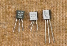
Thanks for pointing me to look into the 5087. Turns out I have some of them here.
Recapping... while the A733 was better than the A1015, I could tell there was still room for improvement. Enter the 2N5087.
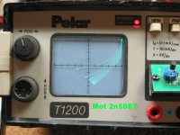
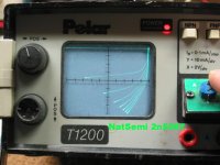
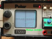
I have 6ea units from Motorola and NatSemi, pulled from various HP gear. Frankly, neither of them look anywhere near "linear" on the curve tracer. And nothing like the data sheet. Maybe they're linear with uA inputs, but not at 100uA and up. There was also a big discrepancy between the transistor tester's Hfe report and what the curve tracer was showing. More on that later. Then I found a bag of some NOS Philips 5087's. Much better. Actually resembles the Mot data sheet.So I took 2 that matched, and installed them.
With 4k7 on the input it sound clearer but still thin. On a whim, I changed the input R to 3k9, which was a step in the right direction. It had enough impact that I had to look further into it.
To see the effects of the base current levels (via series R), I measured 1kHz distortion, from 4k7 on down. by By 3k5 or so I could see H2 and the weed-like packet of higher-order harmonics (H5-H9) lowering. By 2k it started rising again, so the sweet spot was around 2k5 to 2k7.
Installed 2k7's and did some listening. The sound is delicious. Best yet. H2 now sits at -86dB re: 2VRMS.
So it seems to me than the choice of transistor depends on input signal levels, and the base current level as determined by input resistance. Quite significant changes can be made by simply optimizing the latter.
Some data sheets provide useful info to help with this, in the iC vs Vce plots at various base current inputs. But most do not; the 2SA1015 plots start at 200uA input.
Life happens, I have to resume this discussion later.
Attachments
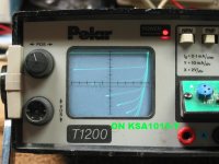
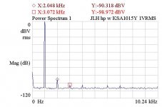
A Digikey box just arrived, with ON Semi KSA1015-Y and KSA992F PNP's inside. Curves are attached. (BTW, Vce for the input transistor in this amp is -9,5V, so we can use the center vertical graticule line for determining gain.)
The 992 looks like it is for very small-signals only. The 1015 looks quite good for this use. Linearity is better than the Toshiba versions at max 200uA or so input (see their tracer plots a few posts back).
Here's how I have been approaching this. For comfortably-loud levels in my various headphones, voltage at the pot wiper is from 66mV to 200mVRMS. The one I like/use most is around 125, so I've used that figure. So 125 x 2.8 = 350mV P-P, divided by 3700 Ohms input resistance (pot + series R) = 95uA max at the base. That's close enough to the 100uA 1st sweep of the tracer. Double that for the more-voltage-hungry 'phones, and we're at the second sweep line. So it's the area between the baseline and those first two sweeps that we want linearity to be the best.
Given all the above, it surprises me is that the high-Hfe transistors (including the 5087) sound good at all.
The KSA1015-Y looks made for the job. It is quite good up to the 2nd sweep. (This is exactly what its data sheet curves show, as well.) And the 2k7 input R appears to be just right, so I'm going to install a pair and listen.
This will be the battle of "high-linearity vs high-Hfe on the input" test. Should be interesting. More later.
Attachments
First to correct some errors.
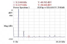
1. Why have there been such small incremental change in distortion measurements, when the audible change was not subtle? I found the answer. It's the programmable preamps of my analyzer. (They are the main reason I keep using this thing; 2dB steps from 1mV to 10VRMS) . In the past I've mostly used the 1V range for testing distortion, and harmonics are down -95 to -96dB from full-scale. But on the 2V range, where I've been testing this amp, they are only -88 re FS, a full 8dB worse. Since decibels don't add linearly, each lowering has been understated.
2. There was no need to be testing at 2VRMS. My fave headphones have 96dB/V sensitivity, and I rarely if ever listen that loud. As I wrote earlier, normal full-code voltage at the pot wiper for comfortably-loud listening levels with these 'phones is 125mV. The amp is 4x gain, so 0.5VRMS = 90dB SPL is my normal max. So I should be testing at 1V or lower anyway.
For continuity, I have posted the 1kHz distortion at 2V (down another .75dB from the A733) and another at 1V. At 1V out, H2 is at -90dB. Which, given what I'm hearing, makes more sense. And, with a -96dB floor, it is actually lower than that. My equipment is the limiting factor here.
I began feeling "bench burnout" today, so I'm gonna take a break for a couple days before testing for optimum source impedance. I'm really liking the amp as it is.
Attachments
There's so much to present here, I've decided to compact it as much as possible.
What I'm examining is the impact of limiting the current being shoved into the base of the input BJT, which is now a KSA1015-Y. I.e. finding the optimum source resistance. When I did this with the 2N5087, it was easy to find by watching the 1kHz harmonics and finding their minima.
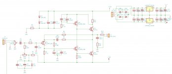
A recap of the setup: 2VRMS source is attenuated 8X (-18dB) through a 10k pot, then a series resistor into the input transistor base, with 82pF to ground there for RF filtering. The amp output is 1VRMS into 300 Ohms, taken through 75 Ohms into the analyzer input.
The pot adds 1k series R.
2VRMS / 8 = 250mV.
250 x 2.8 = 700mV P-P.
700 / 1000 Ohms = 700uA.
This is WAY more than optimum base current for any high-beta PNP I have examined. If the pot wasn't there, it would be even higher.
The schematic has a 4k7 input resistor, which gives 120uA. There must be some other factor(s) coming into play with that high a source R; for every input transistor I've tested, that is too much, and makes the sound "smooth but thin".
The KSA1015 data sheet, and the curve tracer plots, both suggest something in the 200-250uA or so range would be good.
So how much additional series R should be added, for lowest distortion? Let's measure and see what we find.
I ran 1kHz distortion tests using 8 different values of input R; 0R, 1k, 2k, 2k5, 2k8, 3k6, 4k0, and 4k7. Put markers on the first 10 harmonics and looked for patterns to emerge.
It turned out not to be quite as easy with the KSA1015 as it was with the 2N5087, I think because the KSA1015 is more linear in this Ib range. Individual harmonics only varied by 1 to 4dB.
Rather than post all the graphs, I'll boil it all down and highlight the patterns that emerged. (Hx values are individual harmonics, other values are the input resistor)
: H2 was highest at 0K and 1K, fell -1dB to a minimum at 2k8, and stayed around there to 4k7
: If H2 dropped, H4 always rose by about the same amount. Curious.
: H5 - H10 were highest at 0K, fell to a minimum from 2k8 to 3k6, then slowly started rising again at higher R's.
: Harmonics and general noise above 10kHz were worse at 0k, reduced at 2k0, lowest at 2k8, and started rising again at 4k7.
We see minimums converging somewhere in the 2k0 to 2k8 region. Our optimum source resistance region. Adding the pot's 1k R, that translates into 233uA to 185uA base current, respectively.
So whadya know, there is good agreement between the measurements and what the data sheet and curve tracer shows.
Last night I installed 2k0 resistors and listened. Was up till midnight enjoying it. Definitely less edgy. The warmth, clarity and body in the midrange is wonderful. Not monotonic warmth and body, but warmth and body appropriate for each instrument/voice. Things close-miked were much more obvious, not in a bad way, just clearly so.
Tonight I'm going to install and listen to the 2k8's.
An aside: I'm not convinced that measuring 1kHz distortion is the best way to suss this out. Especially when the results are at the bleeding edge of my gear's capability. But hey it worked, so no complaints.
I'll follow up after the 2k8 listen.
What I'm examining is the impact of limiting the current being shoved into the base of the input BJT, which is now a KSA1015-Y. I.e. finding the optimum source resistance. When I did this with the 2N5087, it was easy to find by watching the 1kHz harmonics and finding their minima.
A recap of the setup: 2VRMS source is attenuated 8X (-18dB) through a 10k pot, then a series resistor into the input transistor base, with 82pF to ground there for RF filtering. The amp output is 1VRMS into 300 Ohms, taken through 75 Ohms into the analyzer input.
The pot adds 1k series R.
2VRMS / 8 = 250mV.
250 x 2.8 = 700mV P-P.
700 / 1000 Ohms = 700uA.
This is WAY more than optimum base current for any high-beta PNP I have examined. If the pot wasn't there, it would be even higher.
The schematic has a 4k7 input resistor, which gives 120uA. There must be some other factor(s) coming into play with that high a source R; for every input transistor I've tested, that is too much, and makes the sound "smooth but thin".
The KSA1015 data sheet, and the curve tracer plots, both suggest something in the 200-250uA or so range would be good.
So how much additional series R should be added, for lowest distortion? Let's measure and see what we find.
I ran 1kHz distortion tests using 8 different values of input R; 0R, 1k, 2k, 2k5, 2k8, 3k6, 4k0, and 4k7. Put markers on the first 10 harmonics and looked for patterns to emerge.
It turned out not to be quite as easy with the KSA1015 as it was with the 2N5087, I think because the KSA1015 is more linear in this Ib range. Individual harmonics only varied by 1 to 4dB.
Rather than post all the graphs, I'll boil it all down and highlight the patterns that emerged. (Hx values are individual harmonics, other values are the input resistor)
: H2 was highest at 0K and 1K, fell -1dB to a minimum at 2k8, and stayed around there to 4k7
: If H2 dropped, H4 always rose by about the same amount. Curious.
: H5 - H10 were highest at 0K, fell to a minimum from 2k8 to 3k6, then slowly started rising again at higher R's.
: Harmonics and general noise above 10kHz were worse at 0k, reduced at 2k0, lowest at 2k8, and started rising again at 4k7.
We see minimums converging somewhere in the 2k0 to 2k8 region. Our optimum source resistance region. Adding the pot's 1k R, that translates into 233uA to 185uA base current, respectively.
So whadya know, there is good agreement between the measurements and what the data sheet and curve tracer shows.
Last night I installed 2k0 resistors and listened. Was up till midnight enjoying it. Definitely less edgy. The warmth, clarity and body in the midrange is wonderful. Not monotonic warmth and body, but warmth and body appropriate for each instrument/voice. Things close-miked were much more obvious, not in a bad way, just clearly so.
Tonight I'm going to install and listen to the 2k8's.
An aside: I'm not convinced that measuring 1kHz distortion is the best way to suss this out. Especially when the results are at the bleeding edge of my gear's capability. But hey it worked, so no complaints.
I'll follow up after the 2k8 listen.
And the winner is... I'm not sure. I like them both; and they're very different. With the 2k0 the midrange details get enhanced/pulled forward in a very impressive, enticing way. But I'm not convinced it is the transparent state of things; it's similar to what the 2N5087 was doing.
With the 2k75, the sound is smoother, cleaner, warmer overall, more "of a piece", tonal balance is closer to what I'd expect, just more open and spacious. Maybe there's a different measurement that will help determine which is the more "honest", or something in between. The fact that the higher harmonics and hash were lower with this value incline me toward it.
This little phase has been an enlightening experiment.
As to the choice, it's a terrible problem to have, eh")
With the 2k75, the sound is smoother, cleaner, warmer overall, more "of a piece", tonal balance is closer to what I'd expect, just more open and spacious. Maybe there's a different measurement that will help determine which is the more "honest", or something in between. The fact that the higher harmonics and hash were lower with this value incline me toward it.
This little phase has been an enlightening experiment.
As to the choice, it's a terrible problem to have, eh
Last edited:
Mark Johnson started a thread in the Solid State form, where he and a couple other guys posted Hfe vs Ic for a number of small-signal PNP's. The 2N4403 curve caught my eye, looking very linear at <10mA Ic. Which surprised me because the ones I have tested looked ok but not great, with 300+ Hfe and the nonlinearity that seems to bring with it.
So I went thru my boxes again and found a few more 4403's. One was a bag of NOS Fairchilds from the late 90's. They were all in the 175-225 Hfe range, and linearity on the 200-ish ones looked quite good up to 300uA Ib at 10V Vce, with clean traces and no "loops" on the return sweep. That's 50% more than the KSA1015Y, and would allow a lower series R, hence lower noise and more signal current through the device.
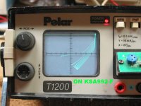
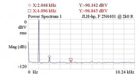
So last night I selected a couple that had around 200 Hfe (1st pic), installed them, and listened briefly. Series R was 2k37, the lowest the KSA's would tolerate. I was tired, it was late, sound seemed cleaner, so went to bed and picked up again this morning.
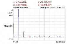
Decided to measure first. H2 was about the same as the 1015, but H3 and H5 had disappeared into the noise floor, and H7-10 all but gone. This cleanup was an eyeopener. Going thru the same procedure as with the 1015, I found the optimum source resistance (by distortion minimum). With all the high-freq garbage gone, it was actually easier to see, at around 1k8 to 2k1 series R. Noise floor also cleans up with the lower source R. (2nd pic)
Installed 2k0 R's and the sound is superb. This is now in what I'd call "world class" territory. The best HP amp I've ever heard.
BTW, subtracting the H2 system residual of -95dB from the -90.4dB measured reading gives the actual value of -98.1dBr.
So I'd say this approach of choosing the input transistor by coordinating max input signal level, device linearity extension, and optimizing the source R to them absolutely works, and handily beats the uber-high-beta devices for sound quality. And yes, there is some wry satisfaction that comes from having a 25-YO 2N4403 beating 'em all... who woulda thunk it...
So I went thru my boxes again and found a few more 4403's. One was a bag of NOS Fairchilds from the late 90's. They were all in the 175-225 Hfe range, and linearity on the 200-ish ones looked quite good up to 300uA Ib at 10V Vce, with clean traces and no "loops" on the return sweep. That's 50% more than the KSA1015Y, and would allow a lower series R, hence lower noise and more signal current through the device.
So last night I selected a couple that had around 200 Hfe (1st pic), installed them, and listened briefly. Series R was 2k37, the lowest the KSA's would tolerate. I was tired, it was late, sound seemed cleaner, so went to bed and picked up again this morning.
Decided to measure first. H2 was about the same as the 1015, but H3 and H5 had disappeared into the noise floor, and H7-10 all but gone. This cleanup was an eyeopener. Going thru the same procedure as with the 1015, I found the optimum source resistance (by distortion minimum). With all the high-freq garbage gone, it was actually easier to see, at around 1k8 to 2k1 series R. Noise floor also cleans up with the lower source R. (2nd pic)
Installed 2k0 R's and the sound is superb. This is now in what I'd call "world class" territory. The best HP amp I've ever heard.
BTW, subtracting the H2 system residual of -95dB from the -90.4dB measured reading gives the actual value of -98.1dBr.
So I'd say this approach of choosing the input transistor by coordinating max input signal level, device linearity extension, and optimizing the source R to them absolutely works, and handily beats the uber-high-beta devices for sound quality. And yes, there is some wry satisfaction that comes from having a 25-YO 2N4403 beating 'em all... who woulda thunk it...
Attachments
Last edited:
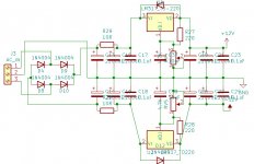
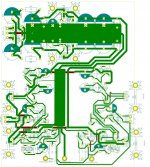
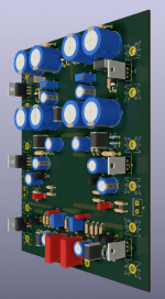
Attempt at improved PCB
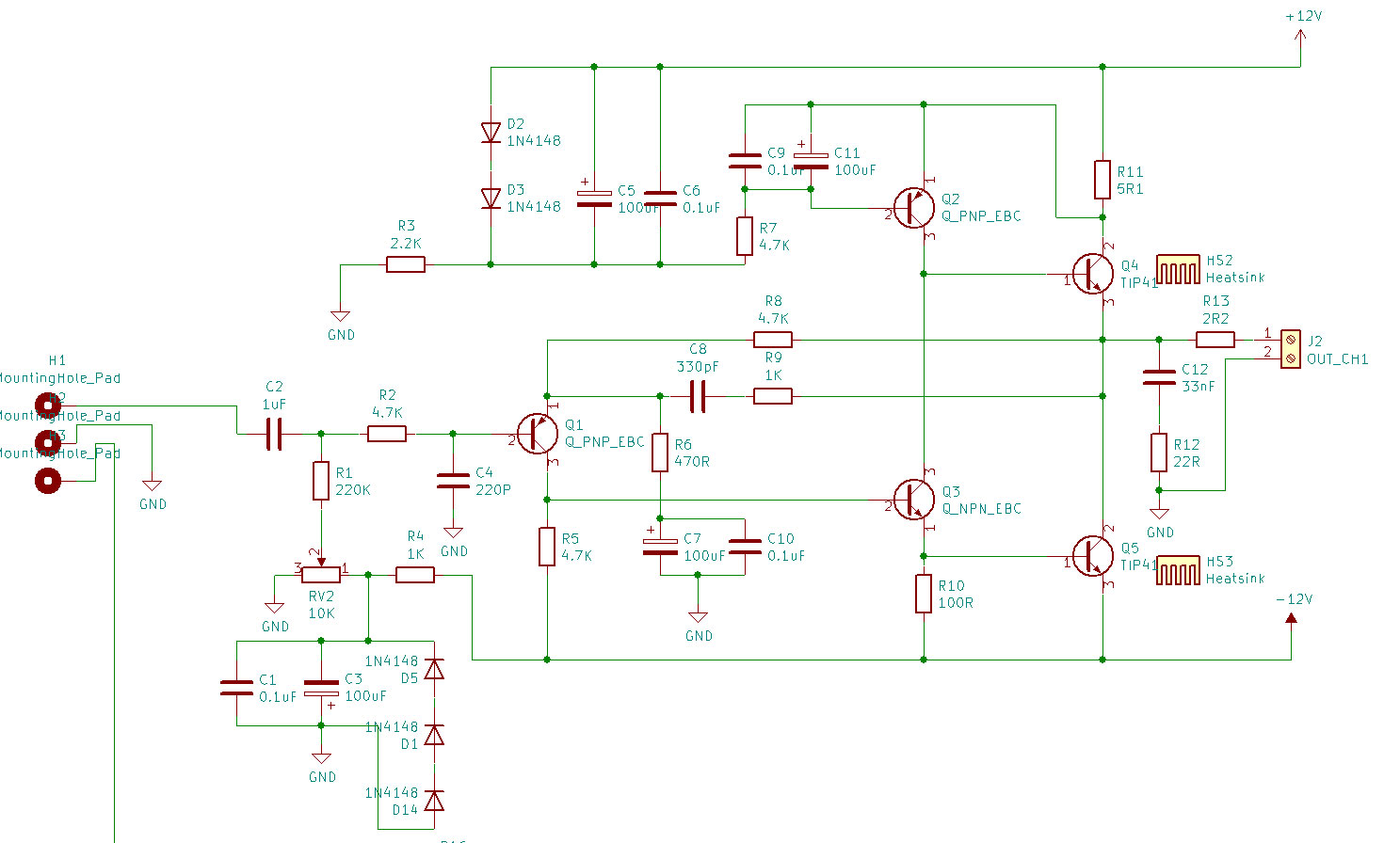
Hi, as i had intended a few post back that i wanted to build my own PCB. So copied the the ebay clone PCB as base, will try to improve it according to this thread. Here is the initial/base PCB (not tested nor built)
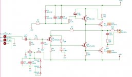
Pls check the schematic and report any bugs.
Hi, as i had intended a few post back that i wanted to build my own PCB. So copied the the ebay clone PCB as base, will try to improve it according to this thread. Here is the initial/base PCB (not tested nor built)
Pls check the schematic and report any bugs.
Attachments
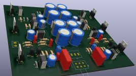
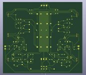
It somewhat looks like a 1-Layer design where the wire jumpers were replaced by a second layer. From taking a quick look at it, you could probably get a more compact and better layout by making better use of the top layer. Are the TO-220s supposed to be mounted to the enclosure?
Are the TO-220s supposed to be mounted to the enclosure?
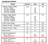
The TIP41's datasheet, see below, says that it can dissipate 2.0 watts with no heatsink, as long as the ambient air temperature is 25 degrees C or less. If the amplifier happens to be located in Dubai where the ambient air temperature is 59 degrees C { =138F }, then the TIP41 can only dissipate (2.0 - (0.016 * (59 - 25) ) ) = 1.45 watts. Still okay.
_
Attachments
I was just wondering why they are positioned in the way they are. If they are supposed to be mounted to the walls of an enclosure, the footprints should move a little close to the board edge. If not, why not move them closer to the other components or why even bother arranging them this way at all? Even if they might not absolutely require a heatsink, you might as well screw them down onto a reasonably sized copper pour when there is this much space available. A free little heatsink and the TO-220s aren't flapping around in the breeze anymore.
It somewhat looks like a 1-Layer design where the wire jumpers were replaced by a second layer.
Yes, it is single layer and i intend to make it single layer to make it diy friendly. It will be using only PTH components.
From taking a quick look at it, you could probably get a more compact and better layout by making better use of the top layer.
Its just base design as i am not an expert in any way and am still learning kicad. Will try to make more compact.
Are the TO-220s supposed to be mounted to the enclosure?
the PCB layout is not final, i will be using separate heatsinks on the TIPs.
Todo list:
Re-design the PCB so that
the ground routes are good and nice
Separate the PSU section /OR better replace it with another PSU
Remove the 2.7v zener and use the 3x diodes / OR
add the DC Servo mentioned in the previous posts.
maybe:
add output delay and DC protect.
Hi,
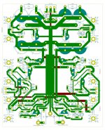
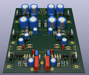
Had some time to work on the PCB. Its not final yet.
Here are the things done so far
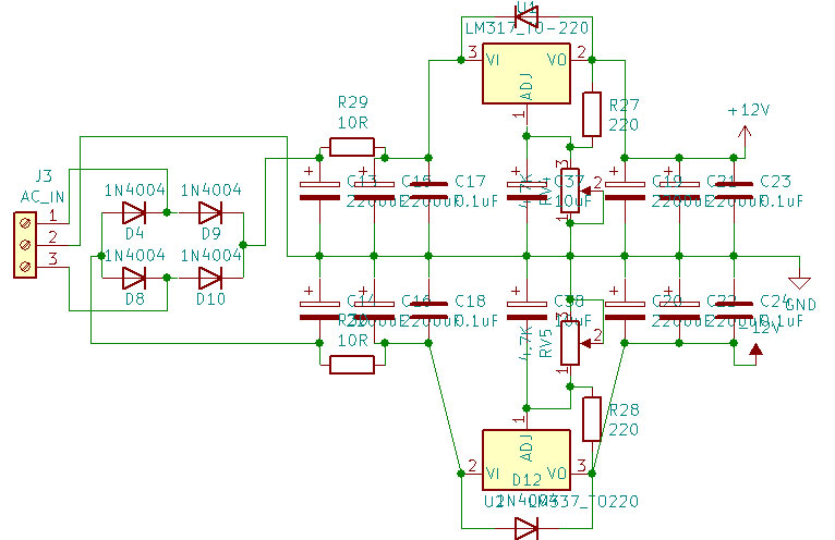
1. The PSU now uses LM3x7 regulators.
2. Attempted at shortest ground path. (needs more work)
3. Replaced Zener with 3x diodes (will replace with DC Servo later)
4. Replaced input screw terminal with Pads
5. Removed the volume POT.
Only left side is done so far. Need tips, suggestions. Is this the right path to go. Or should the PSU be separate from this board ?

Had some time to work on the PCB. Its not final yet.
Here are the things done so far
1. The PSU now uses LM3x7 regulators.
2. Attempted at shortest ground path. (needs more work)
3. Replaced Zener with 3x diodes (will replace with DC Servo later)
4. Replaced input screw terminal with Pads
5. Removed the volume POT.
Only left side is done so far. Need tips, suggestions. Is this the right path to go. Or should the PSU be separate from this board ?
Attachments
Some basic suggestions:
: Remove C8, C9, C10, R9. Not needed.
: Replace R13 with jumper. Ditto.
: Increase C2 to at least 3.3uF
: Increase C7, C11, C30, C37 to 470uF.
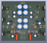
I would rethink the layout geometry between supply and circuit. Consider what nigel pearson has eloquently said, even in this thread (post #7012); "Don't forget, an amplifier is a signal modulated power supply."
You've gone through a lot of trouble to create a low-noise and (supposedly) low-impedance power supply, but then connected it to the circuit via long, thin traces, which add considerable resistance and inductance to them. This more than triples their output impedance at low freqs, and much worse at high freqs. A major priority of the layout has to be maintaining low impedance for the rails and ground.
Also, look at the photo in post #888. See the cuts in the ground trace between filter and regulator sections, which force the ground currents to mix before passing on to the regulation.
: Remove C8, C9, C10, R9. Not needed.
: Replace R13 with jumper. Ditto.
: Increase C2 to at least 3.3uF
: Increase C7, C11, C30, C37 to 470uF.
I would rethink the layout geometry between supply and circuit. Consider what nigel pearson has eloquently said, even in this thread (post #7012); "Don't forget, an amplifier is a signal modulated power supply."
You've gone through a lot of trouble to create a low-noise and (supposedly) low-impedance power supply, but then connected it to the circuit via long, thin traces, which add considerable resistance and inductance to them. This more than triples their output impedance at low freqs, and much worse at high freqs. A major priority of the layout has to be maintaining low impedance for the rails and ground.
Also, look at the photo in post #888. See the cuts in the ground trace between filter and regulator sections, which force the ground currents to mix before passing on to the regulation.
Last edited:
DoneSome basic suggestions:
: Remove C8, C9, C10, R9. Not needed.
Leaving it as is for now. I think it was mentioned in the DC Servo mod to change to 68ohms: Replace R13 with jumper. Ditto.
Done: Increase C2 to at least 3.3uF
C7, C11 Done: Increase C7, C11, C30, C37 to 470uF.
Cant locate C30 and C37
I would rethink the layout geometry between supply and circuit. Consider what nigel pearson has eloquently said, even in this thread (post #7012); "Don't forget, an amplifier is a signal modulated power supply."
You've gone through a lot of trouble to create a low-noise and (supposedly) low-impedance power supply, but then connected it to the circuit via long, thin traces, which add considerable resistance and inductance to them. This more than triples their output impedance at low freqs, and much worse at high freqs. A major priority of the layout has to be maintaining low impedance for the rails and ground.
Also, look at the photo in post #888. See the cuts in the ground trace between filter and regulator sections, which force the ground currents to mix before passing on to the regulation.
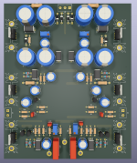
Have tried to reduce the length of tracks, but i think its not the best way to do it. Have not built it yet. Will refine it a bit more then will go for first proto
If anyone can make it perfect, i will share the kicad project. As i am still learning kicad while fiddling with this.
Attachments
{R13} Leaving it as is for now. I think it was mentioned in the DC Servo mod to change to 68ohms.
That would not be good...
Cant locate C30 and C37
They're the caps from both regulator's adjust terminal to ground, currently 10uF.
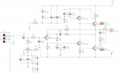
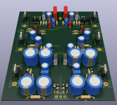
That layout looks much better.
A couple more things: R2 is too high a source impedance for most BJT transistors, especially if there is a pot preceeding it. Something in the 1k to 2k range would be better. And C4 can be lowered to 100pF.
What are you using for Q1, Q2, and Q3?
- Home
- Amplifiers
- Headphone Systems
- JLH Headphone Amp