^ You are referring to D1 and D2 on the JLH Circuit 1 schematic, I guess?
Correct. I'll try to termally couple the TRs and the diodes and see what happens.. Thanks for your deailed answer.

Hi Guys,
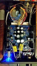
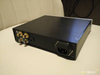
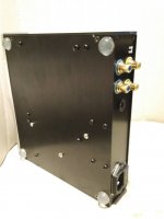
Today I have fulle completed the JHL headamp according to my initial plans. I've added a little circuit that protects the headphones from DC + a separate dedicated PSU. A nice feature of this PCB is that has a little delay circuit as well, so the servo has some time to settle, minimising DC before any signal is conducted to the headphones. It also inmidiately switches off the relay when the amp is switched off, so no switch noises are transmitted. Of course this board is modified as well, according to some of the suggestions posted here:
Headphone protector | Rock Grotto
I am pretty statisfied with the result
.JPG)
.JPG)
Hi Kaplaars,
great work. Thanks for all your information about the jlh-headphone-amp-kit and tunig methods. I hope you are still active in this forum.
Could you explain why you use a separat power-supply for the headphone-protection-unit. I want to build a headphone amplifier based on the kits and find the protection unit very useful. what's the downside, when I connect the unit directly to the main power supply.
Regards
Schiller72
High dc offset
Hi Ashok,
Fair enough, The schematic is on thread # 119 (milescampble). I must have done something accidentally while trying to get to the sources of the hum, the channel is producing -5.71V of DC offset compared to 14mV in the other.
I have checked the transistors and they seem to be ok. Can you suggest a strategy to remedy this?
Thanks
RF
Attachments
With the changes you made you should get about -1.6V or so at the emitter of the input transistor Q5/Q6 . Your Q7 collector is at -5.08 v. At this voltage Q5 should be cut off and it doesn't appear to be so.
Replace Q5 with another PNP like BC556B/BC560B.BC558B etc. Check the terminal orientation. I think it's the same as 2N2907 , but double check it. Then try again.
Your second channel Q4/Q10 appears to be OK. Also check the input dc bias diodes of the bad channel . If one diode is reversed you will get a -V at the output or Q7 collector.
High DC offset
Changed Q5 with BC558b. Biasing diodes are in correct formation.
Q5 readings with respect to GND is as follows:
E: -5.73 B: -2.0 C: -10.61
Values on Q1,Q7,Q3,Q4,Q9 are same as prior.
DC offset still remains at -5.73V. What do you suggest I do next?
Thanks,
RF
Changed Q5 with BC558b. Biasing diodes are in correct formation.
Q5 readings with respect to GND is as follows:
E: -5.73 B: -2.0 C: -10.61
Values on Q1,Q7,Q3,Q4,Q9 are same as prior.
DC offset still remains at -5.73V. What do you suggest I do next?
Thanks,
RF
Check voltage ( with respect to ground) at the top of VR3 on both channels. It should be about -2.4V .
Check the voltage at the base of the input transistors Q5 and Q6. It should be about -2.13 V.
In the simulation if R5 ( 4.7K ) is removed the output should be + 5.71 V. Opposite of what you get.
I tried reversing all transistors one by one. None produce -5.73V or anything close to it. It stays positive.
Check if C23/C17 the feedback capacitor ( 180uF) is leaky or reverse connected !
Do the following.
1. Inspect the input stage of both channels. Measure the resistors in circuit and ensure it is the same on both boards.
2. Check the transistor orientation on both boards by measuring the base/coll/emitter diode direction.
3. Make sure that the tracks are not cut or anything which makes them different. Check for a thin faulty trace or track to track short.
4. Compare Q5/Q6 voltages.
If Q5 base is -2V , then the emitter should be -1.6 under normal circumstances.
Exchange transistors between boards and test each time. Like Q1 and Q2 , Q3 / Q4 etc. After each change check if the problem shifts to the other board. If so that part is bad ....and the good board will now have the problem.
Last edited:
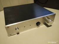
Hi! I used 2204E Headphone Chassis Full Aluminum Preamplifier Enclosure Amp Box PSU Case | eBay for my JLH Headphone amp.
The sound of this amp is warm and clear sound. The best
quality of sound is 2 hours after power on of this amp.
The sound of this amp is warm and clear sound. The best
quality of sound is 2 hours after power on of this amp.
Attachments
Sorry for the Noob question. Can someone help me with the specifications for the toroidal transformer ? Believe spec is 15v-0-15v what is the amperage or volt-ampere ?
Planning on buying from Antek
Bought the ZeroZone JLH Headphone Amp
Thank you !
Planning on buying from Antek
Bought the ZeroZone JLH Headphone Amp
Thank you !
Sorry for the Noob question. Can someone help me with the specifications for the toroidal transformer ? Believe spec is 15v-0-15v what is the amperage or volt-ampere ?
Planning on buying from Antek
Bought the ZeroZone JLH Headphone Amp
Thank you !
Great amp, but keep in mind you'll have high DC offset without a servo.
Great amp, but keep in mind you'll have high DC offset without a servo.
Thank you ammel68. Thought is to first build the amp then add DC Servo think this is the PCB
Can you assist with specifying the Antek Transformer ?
Thank you !
Hi Kaplaars,
great work. Thanks for all your information about the jlh-headphone-amp-kit and tunig methods. I hope you are still active in this forum.
Could you explain why you use a separat power-supply for the headphone-protection-unit. I want to build a headphone amplifier based on the kits and find the protection unit very useful. what's the downside, when I connect the unit directly to the main power supply.
Regards
Schiller72
Hi Schiller72,
Sure! The reason why I used a separate transformer + 7812 regulator is that otherwise a groundloop would have been created which results into hum. Ergo, the protection unit works best with a separate PSU
") .
.Regards,
Michael
Hi Schiller72,
Sure! The reason why I used a separate transformer + 7812 regulator is that otherwise a groundloop would have been created which results into hum. Ergo, the protection unit works best with a separate PSU
Regards,
Michael
Thanks for the answer Kaplaars. Now i understand the reason for the seperat PSU.
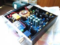
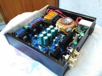
Groundloops often makes trouble (i know the problem).I'm building the JLH amplifier based on ebay PCB at the time (see following photos).
Note: I use a separate power supply and a separate input stage (loudness control). Therefore, the bridges on the JLH-PCB.
An externally hosted image should be here but it was not working when we last tested it.
An externally hosted image should be here but it was not working when we last tested it.
I also have some problems with the dc offset.
My idea was the two power transistors (Q3 and Q9 / Q4 and Q10) (all TIP41) thermally couple. Furthermore, the 2.7 volt zener diode have replaced with 4x 1N4148. These four diodes are also thermally connected with the heatsink. The temperature dependence of diodes and transistors counteract, so that actually a more stable (smallest possible) DC offset should occur. But my measurements show a not so good performance. I ask myself why.
Start // DC_Offset: +64 mV
30 sec. // DC_Offset:. +30 mV
after 2 min. // DC_Offset: -2 mV
after 4 min. // DC_Offset: -4.5 mV
after 8 min. // DC_Offset: -6 mV
after 10 min. // DC_Offset: -8 mV
after 14 min. // DC_Offset: -12 mV
another measurement cycle
Switching // DC_Offset: +28 mV // heatsink: 15 °C
after 20 sec. // DC_Offset. -5 mV
after 1 min. // DC_Offset: - 15mV
after 30 min. // DC_Offset: approx. +/- 1.5 mV (cyclic rise and fall) // headsink: 51 °C
This is not so bad but not ideal. Also not always reproducible. Each measurement cycle gives slightly different values.
What are the values of the active OPA based DC-servo-control (OPA as integrator) ?
Can anyone possibly help my variant of the thermal coupling (diodes / output transistors) to improve?
Thanks for any comments or tips.
Regards
Schiller72
Last edited:
Thank you ammel68. Thought is to first build the amp then add DC Servo think this is the PCB
Can you assist with specifying the Antek Transformer ?
Thank you !
You're quite welcome! Yes, that's the servo board I offer for these amps.
I've been using a Rat Shack 12.6V-0-12.6V 2A transformer.
If I were getting an Antek, I would get this one:
AS-1212 - 100VA 12V Transformer - AnTek Products Corp
Hope that helps.
I also have some problems with the dc offset.
My idea was the two power transistors (Q3 and Q9 / Q4 and Q10) (all TIP41) thermally couple. Furthermore, the 2.7 volt zener diode have replaced with 4x 1N4148. These four diodes are also thermally connected with the heatsink. The temperature dependence of diodes and transistors counteract, so that actually a more stable (smallest possible) DC offset should occur. But my measurements show a not so good performance. I ask myself why.
Start // DC_Offset: +64 mV
30 sec. // DC_Offset:. +30 mV
after 2 min. // DC_Offset: -2 mV
after 4 min. // DC_Offset: -4.5 mV
after 8 min. // DC_Offset: -6 mV
after 10 min. // DC_Offset: -8 mV
after 14 min. // DC_Offset: -12 mV
another measurement cycle
Switching // DC_Offset: +28 mV // heatsink: 15 °C
after 20 sec. // DC_Offset. -5 mV
after 1 min. // DC_Offset: - 15mV
after 30 min. // DC_Offset: approx. +/- 1.5 mV (cyclic rise and fall) // headsink: 51 °C
This is not so bad but not ideal. Also not always reproducible. Each measurement cycle gives slightly different values.
What are the values of the active OPA based DC-servo-control (OPA as integrator) ?
Can anyone possibly help my variant of the thermal coupling (diodes / output transistors) to improve?
Thanks for any comments or tips.
Regards
Schiller72
As I've stated before, these amps are NOTORIOUS for constantly fluctuating and high DC-offset.
You can go to the trouble of thermal coupling different components and you're still going to have high and fluctuating offset.
A simple servo will take care of it. My examples stay within a couple of millivolts.
- Home
- Amplifiers
- Headphone Systems
- JLH Headphone Amp