This is the GB thread for Keantoken's Aurum-X 300w Class AB amplifier. The technical discussion for this amp is here:
Keantoken's Aurum-X 300w Amp with LatFETs
Schematic of prototype:
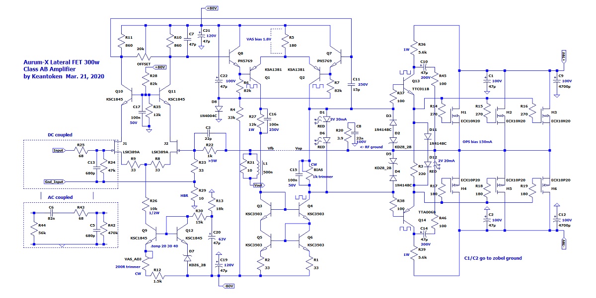
Full schematics of the prototype here:
Front End Mezzanine board
Main Board
BOM here.
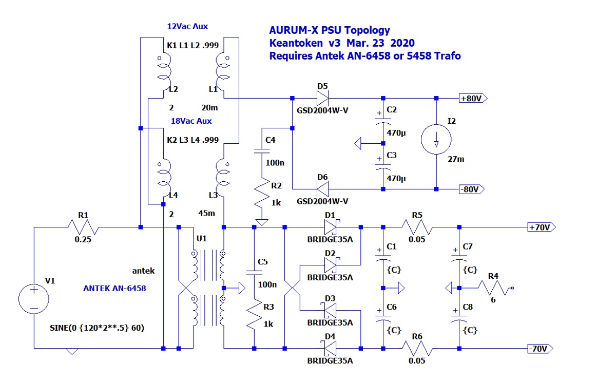
Power Supply will be an Antek AN-5458 or AN-6458 trafo for each channel, which provides +/-70v for the power latFETs and +/-80v for the front-end mezzanine board:
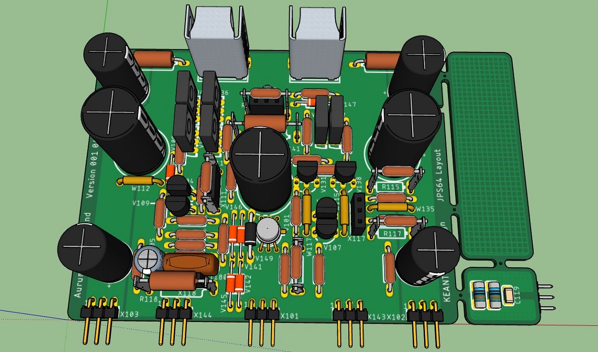
This is a 3d render of the front end (FE) mezzanine board:
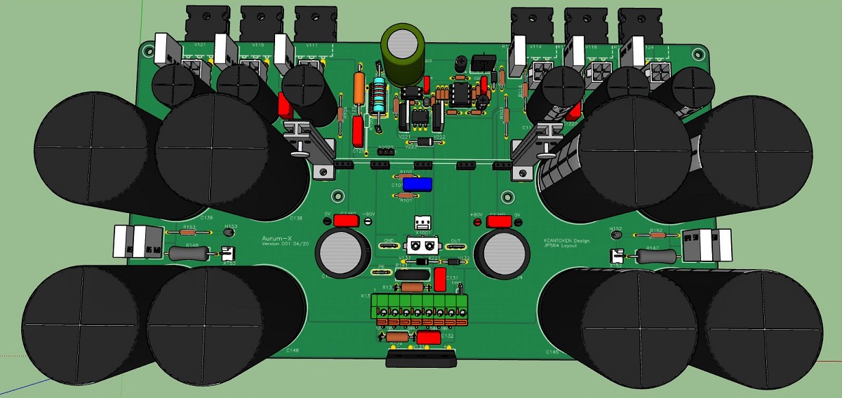
Here is a 3d render of the main board which is 275mm x 150mm:
This amp is an advanced level project to be sure involving high voltages (+/-80v and +/-70v) at high currents, and a high level of complexity. It is also a high cost project given that there are 16x 10,000uF 100v capacitors for the main power supply ($14ea), two 600VA trafos at $67ea, and a dozen Exicon S-grade lateral MOSFETs with 8 spares at about $200. The PCBs themselves are huge and expensive being 275mm x 150mm, 2mm thick, 2oz copper, and ENIG.
For a chassis, something along the lines of a 5U x 300mm will be minimum - probably 4U x 400mm would work better as there is more room for the dual trafos. On the bright side, the CRC PSU is self contained on the PCB, as is the SSR for DC protection. So the chassis floor is fully wide open for the taking. I will try to make it fit in a 4U x 300mm chassis where my Alpha Nirvana currently resides. I will or that amp to a new chassis that is on the way. Assuming 300w contiguous operation, the heatsink will need to reject 114w per channel. However, most people would rarely play this at more than 50w in a domestic environment so heatsink sizes might be a lot more modest.
I will need interest for at least 5 stereo board-sets (2 main and 2 mezzanine). Cost of stereo board-sets will be $95. Yes, the cost is high, but this is a special amp with a storied past and legendary performance based on the predecessor commercial amp with which it was inpsired by. Given that it has been 10 years in the works as an LTspice optimization exercise by Keantoken, and now superbly laid out by JPS64, a professional master designer - I think it may even surpass it's progenitor.
Do you have what it takes to buid the Aurum-X? You have to ask yourself: "How badly do I want this??!!!!"")
I would like to thank Keantoken and JPS64 for agreeing to work with me on this project - you guys are brilliant and I hope to realize this amp soon. It has been a lot of fun collaborating on this and seeing it evolve. But now is the time to start slinging solder and see how it sounds.
Please add your name to the list if you think you are up to the task of building what has been called "The Very Best Amplifier I Have Ever Heard!"
4 more to go...
Keantoken's Aurum-X 300w Amp with LatFETs
Schematic of prototype:
Full schematics of the prototype here:
Front End Mezzanine board
Main Board
BOM here.
Power Supply will be an Antek AN-5458 or AN-6458 trafo for each channel, which provides +/-70v for the power latFETs and +/-80v for the front-end mezzanine board:
This is a 3d render of the front end (FE) mezzanine board:
Here is a 3d render of the main board which is 275mm x 150mm:
This amp is an advanced level project to be sure involving high voltages (+/-80v and +/-70v) at high currents, and a high level of complexity. It is also a high cost project given that there are 16x 10,000uF 100v capacitors for the main power supply ($14ea), two 600VA trafos at $67ea, and a dozen Exicon S-grade lateral MOSFETs with 8 spares at about $200. The PCBs themselves are huge and expensive being 275mm x 150mm, 2mm thick, 2oz copper, and ENIG.
For a chassis, something along the lines of a 5U x 300mm will be minimum - probably 4U x 400mm would work better as there is more room for the dual trafos. On the bright side, the CRC PSU is self contained on the PCB, as is the SSR for DC protection. So the chassis floor is fully wide open for the taking. I will try to make it fit in a 4U x 300mm chassis where my Alpha Nirvana currently resides. I will or that amp to a new chassis that is on the way. Assuming 300w contiguous operation, the heatsink will need to reject 114w per channel. However, most people would rarely play this at more than 50w in a domestic environment so heatsink sizes might be a lot more modest.
I will need interest for at least 5 stereo board-sets (2 main and 2 mezzanine). Cost of stereo board-sets will be $95. Yes, the cost is high, but this is a special amp with a storied past and legendary performance based on the predecessor commercial amp with which it was inpsired by. Given that it has been 10 years in the works as an LTspice optimization exercise by Keantoken, and now superbly laid out by JPS64, a professional master designer - I think it may even surpass it's progenitor.
Do you have what it takes to buid the Aurum-X? You have to ask yourself: "How badly do I want this??!!!!"
I would like to thank Keantoken and JPS64 for agreeing to work with me on this project - you guys are brilliant and I hope to realize this amp soon. It has been a lot of fun collaborating on this and seeing it evolve. But now is the time to start slinging solder and see how it sounds.
Please add your name to the list if you think you are up to the task of building what has been called "The Very Best Amplifier I Have Ever Heard!"
Name / Stereo-Board-Sets / Country
xrk971 / 1 board set / USA
4 more to go...
Attachments
Last edited:
X,
Looks like quite an "epic" project!
4U x 300 mm / 4U x 400 mm is common for DIY Class A builds. IMHO good call with integrating the CRC PSU on to the main amplifier board - will keep the floor of the chassis clean, and also the proximity of the capacitors should have some benefits too I guess.
Looks like quite an "epic" project!
4U x 300 mm / 4U x 400 mm is common for DIY Class A builds. IMHO good call with integrating the CRC PSU on to the main amplifier board - will keep the floor of the chassis clean, and also the proximity of the capacitors should have some benefits too I guess.
Hi Zman01,
Yes, the idea behind putting the bulk caps on the main PCB is to keep the traces from the caps to the MOSFET drains as short and low-impedance path as possibe for maximum bass authority. Plus, it frees up the amp chassis floor plate to install other things like the trafo's and wiring terminal blocks, etc. Since the PSU CRC and SSR speaker protection circuits are all on the main board, this is actually a simple amp from standpoint of connection of various amp systems together.
Yes, the idea behind putting the bulk caps on the main PCB is to keep the traces from the caps to the MOSFET drains as short and low-impedance path as possibe for maximum bass authority. Plus, it frees up the amp chassis floor plate to install other things like the trafo's and wiring terminal blocks, etc. Since the PSU CRC and SSR speaker protection circuits are all on the main board, this is actually a simple amp from standpoint of connection of various amp systems together.
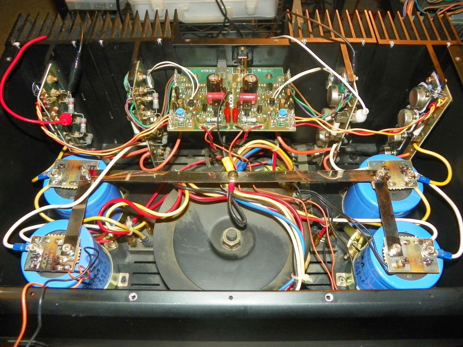
I was looking at the famous Adcom GFA-555 designed by Nelson Pass, and noticed that the output stage power BJTs (all TO-3) were remotely located with flying leads and the front end is on a separate board. However, the PSU rail caps are remotely located. This is a 200w/ch Class AB amp and the amp doesn’t look so intimidating. A lot of manual touch-work spaghetti (DIY like) wiring harnesses on this amp.
Some had the front end board horizontally mounted:
An externally hosted image should be here but it was not working when we last tested it.
Some had the front end board horizontally mounted:
Last edited:
I think Keantoken already answered the question about the diodes on the driver stage. They are correct as shown.
I have placed the order for the prototype verification build PCBs. 2mm, 2oz, ENIG in main board and 1.6mm, 1oz, ENIG on FE board.
Time to start gathering my finances to fund this development project.
The heavy hitters are: rail caps, latFETs, trafos.
I have placed the order for the prototype verification build PCBs. 2mm, 2oz, ENIG in main board and 1.6mm, 1oz, ENIG on FE board.
Time to start gathering my finances to fund this development project.
The heavy hitters are: rail caps, latFETs, trafos.
Last edited:
Time to start gathering my finances to fund this development project.
Ready, steady, go...!
Will watch this thread closely.
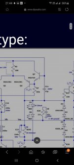
In #1 post, the schematic in https://www.diyaudio.com/forums/att...-amp-latfets-aurum-schematic-v001-ltspice-jpg, is different from the pdf schematic in https://www.diyaudio.com/forums/att...m-300w-amp-latfets-aurum-x_tht_fe_sch_001-pdf.. miss match area is in the VAS stage
So is the PDF schematic correct? Because that is what is being manufactured into the prototype PCB.
https://www.diyaudio.com/forums/att...m-300w-amp-latfets-aurum-x_tht_fe_sch_001-pdf
https://www.diyaudio.com/forums/att...m-300w-amp-latfets-aurum-x_tht_fe_sch_001-pdf
So is the PDF schematic correct? Because that is what is being manufactured into the prototype PCB.
https://www.diyaudio.com/forums/att...m-300w-amp-latfets-aurum-x_tht_fe_sch_001-pdf
no
If would be good if someone can redline a schematic to show exactly what we are talking about. I might have to order another set of FE boards. At least they are small and inexpensive compared to the MB. I guess we need more eyes on the schematics before going to press. This happens on complex projects. Oh well.
Thanks for pointing that out Myl.
Thanks for pointing that out Myl.
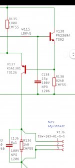
Looks like I have a little surgery to do on the verification boards. Here is what JPS64 suggests:
cut trace from H141 (Anode) to C131 (-)
cut trace from C138 to R138
V141 and R143 equipped on solder side:
do not short V141 (Cathode) lead
do not short R143 lead (opposite side to MOSFET Gate)
solder wire from H141 (Anode) to R136 (trace to V137)
solder wire from H141 (Anode) to C138
solder long lead V141 (Cathode) to H141 (Anode)
solder long lead R143 to H141 (Anode)
Attachments
- Status
- This old topic is closed. If you want to reopen this topic, contact a moderator using the "Report Post" button.
- Home
- Group Buys
- Aurum-X 300w Class AB Amp GB