This is the Group Buy and Build thread for the Alpha Nirvana 39W SE Class A amplifier designed by AKSA.
PCBs:
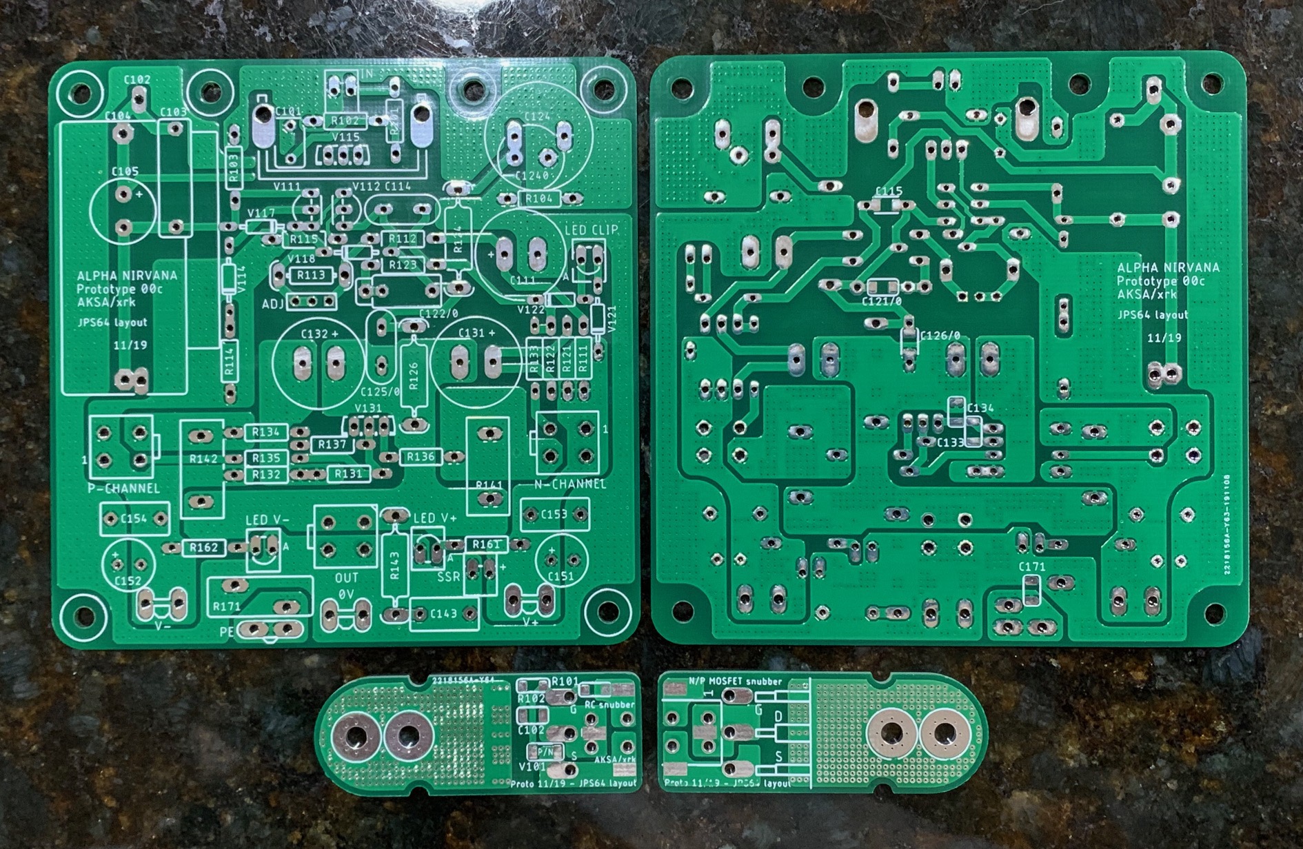
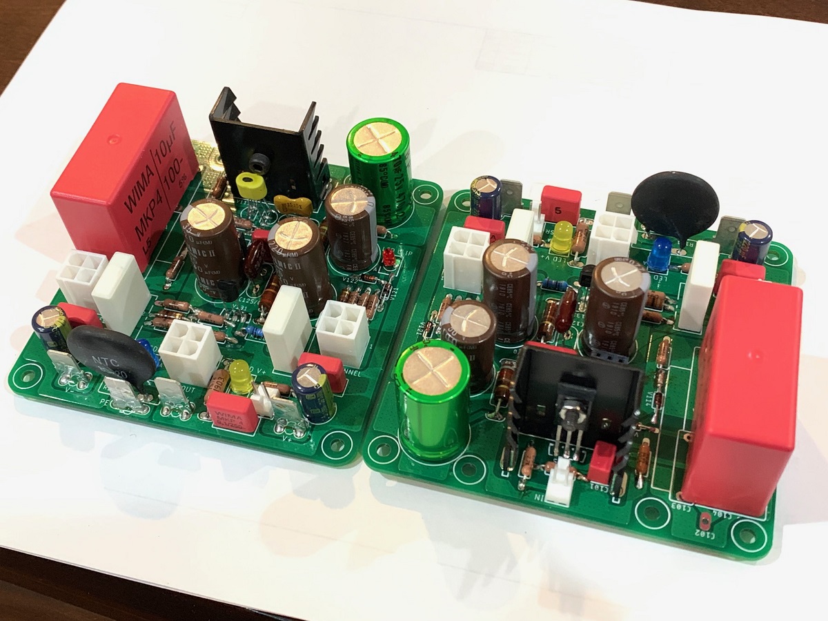
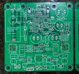
Amp module looks like this assembled:
Hi X,
Comparing the 'built' pic against the PCB pic ... am I right in thinking that only one of C102, 103, 104, 105 gets populated on the PCB?
In your case, the 10uF Wima was used?
Thanks,
Andy
Yes, C102,103,104,105 are all the same input coupling cap. Simply there to give you choices as to what cap package you can use. Yes, I have a 10uF Wima MKP there. A 10uF Silmic II at C105 can work very well and hardly costs anything.
Great - thanks, X.
")
Andy
Hi Sanjeev,
If you like simplicity, please consider the ABBB amp. Very similar to the Alpha Nirvana, but 50w capable and has built in SLB and SSR DC protection and delay circuit. You just need to connect a trafo and speakers. It also has output MOSFETs and Cap Mx BJTs on quick connect Molex for remote mounting.
The Alpha Big Boy with Buttah (ABBB) 52w Class A Amp GB
Here is one channel of Vunce’s build:
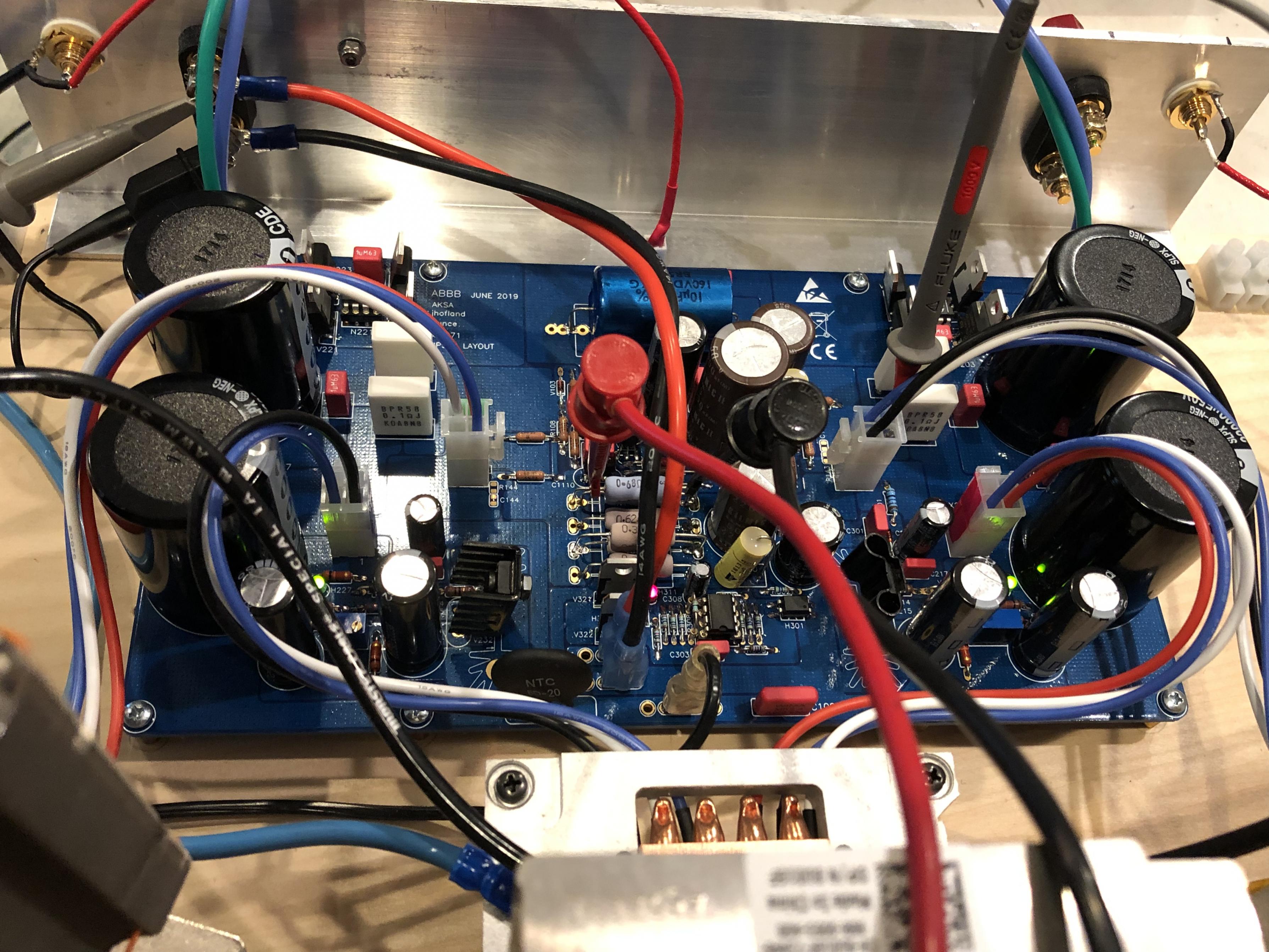
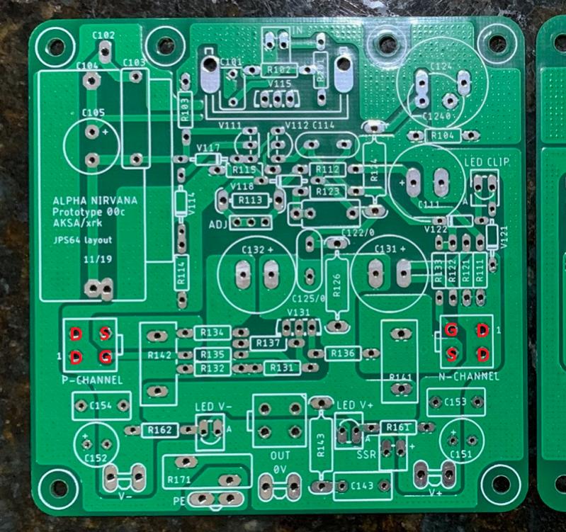
There was a questions about how to wire the Molex quick connects on the PCB. Here is a diagram that should help. Remember that the big white source resistors are connected to the source (S) pins and the power supply is connected to the drain (D) pins. The little trace is the gate (G) pin. This is true for N or P channel. On the MOSFET, the pins left to right are G D S, always, for non-lateral FET MOSFETs.
Attachments
There was a questions about how to wire the Molex quick connects on the PCB. Here is a diagram that should help. Remember that the big white source resistors are connected to the source (S) pins and the power supply is connected to the drain (D) pins. The little trace is the gate (G) pin. This is true for N or P channel. On the MOSFET, the pins left to right are G D S, always, for non-lateral FET MOSFETs.

Thanks, X.
That almost makes sense to me ... but I'm afraid not quite!
Referring to your pic, can you just confirm my understanding is correct; for both MOSFETs, proceeding anti-clockwise:
* the wire to the Drain goes in the hole marked '1'
* the wire to the Gate goes in the next hole, whilst
* the wire to the Source goes in the next hole.
Thanks a lot,
Andy
Correct, note that Drain is double. So from pin 1 on the Molex going CCW D, G, S, D. You can use either D pin.
And note that both N and P channel MOSFETs have pins arranged as G, D, S from left to right looking at the front of the MOSFET (side with markings, amd legs facing down).
And note that both N and P channel MOSFETs have pins arranged as G, D, S from left to right looking at the front of the MOSFET (side with markings, amd legs facing down).
Last edited:
Thanks X, I think I have my head firmly around this after looking at the schematic. the board. and testing the connector nearest resistor. The discrition you give makes it even easier.
Okay. did a little more testing and it appears as though The N channel is working, but there is an issue with the P channel, which, if I don't keep a current limit, will smoke R18 in the SLB. I also noticed that the - rail voltage drops to 4.6 volts when loaded with the P channel MOSFET.
I'm going to replace a slightly toasted R18 on the SLB and run the same test with the other channel of the SLB. I built both of them together, both clamped in the vise and added parts for both board at the same time. If I have some value that is off, or a part wrong way, it should be that way on both. I'll run that test and check results.
That’s a dead short - your P channel MOSFET is either bad (shorted out internally) or you are putting a N channel where there should be a P channel and that will act like a short.
What does an ohm meter show as resistance between D and S? Nothing connected.
Shows 2.2 Meg and open on the reverse.
All I can say is.... YouTube
Thanks to X for all his help here, it's breathing, still have some testing to do and set DC offset, but the values look good.
N-P channels very close in values: Gate 4.7V Drain 27.84V Source= .389V
The bottle of Whiskey goes to Vunce. I'm very glad I saw your post before you deleted it! I didn't know the supply would run at idle if there was a problem with the transistor. I had the G&S reversed on Q12. A great call my friend, let me know where to send the bottle.
I had a 150W bulb in at it lit almost full power, but nothing seemed amiss, so I decided to go to mains with my hand on the cord. After a few moments and nothing exploding or smoking tested and the values were solid,. This draws some amps and that's only one channel.
Last edited:
The bottle of Whiskey goes to Vunce. I'm very glad I saw your post before you deleted it! I didn't know the supply would run at idle if there was a problem with the transistor. I had the G&S reversed on Q12. A great call my friend, let me know where to send the bottle.
Nice job JT!!
When I posted the comment about the SLB Q12, I wanted to double check my notes. So I decided to delete it until I did.
Glad you have success now
Nice job JT!!
When I posted the comment about the SLB Q12, I wanted to double check my notes. So I decided to delete it until I did.
Glad you have success now
I mean to say the B&E reversed.
Thanks again, my first foray into flying leads, I have much better understanding from this one, so all is well.
Good to hear you got it working JT. So the problem was with the SLB and not the Alpha Nirvana?
Yes, that's correct, but in reality, the problem was two feet and to the left behind the soldering iron.
In effect Q12 was not in the circuit, so R18 tried to drop the voltage. .5W resistor isn't going to cut it. lol.
two things, the best place to measure DC offset and should we jump the R133 & R135 having the 100R already on the snubber?
Last edited:
At speaker output is best place to measure DC offset. Yes, jumper the on board snubber resistors if already on snubber board.
That's where I was measuring X, but the resistor (R113) value didn't matter. The DC offset is very low anyway. 7mV and 3mV. Could the snubber resistor be affecting anything with the resistor value on the DC offset?
- Home
- Group Buys
- Alpha Nirvana 39W SE Class A Amplifier GB