In case anyone wants to get the smaller MOSFET snubber boards that were designed for the ABBB amp, they are now available in my shop. A set of 4 (N channel and P channel MOSFET and NPN and PNP BJT) on a single panel for $15.
A member asked that these be made available as he needed a lower profile one than the bigger ones that were used on the Alpha Nirvana.
A member asked that these be made available as he needed a lower profile one than the bigger ones that were used on the Alpha Nirvana.
In case anyone wants to get the smaller MOSFET snubber boards that were designed for the ABBB amp, they are now available in my shop. A set of 4 (N channel and P channel MOSFET and NPN and PNP BJT) on a single panel for $15.
A member asked that these be made available as he needed a lower profile one than the bigger ones that were used on the Alpha Nirvana.
Where/when would the smaller snubber boards be preferable vs the bigger ones? Could the Aleph J be built using these? I guess the AJ PCB doesn't have anywhere for the molex connector though...
I was toying with the idea of building an amp chassis with dual mono SLBs, RTR DC protection boards, and SFP, and ideally be able to swap between the Aleph J, Alpha Nirvana, and other amp boards. Not sure how realistic that is, but I know I can't afford to build a whole PS, chassis, etc for all the DIY Audio amp designs I want to try.
Edit: shoot. now I'm remembering that the Aleph J and Alpha Nirvana use significantly different PCB rail voltages, so maybe this isn't practical. I may have to settle for 1 chassis/PS for Pass / FirtWatt designs, and a second for the AN and others that use higher voltage rails.
The member who asked me about the smaller snubbers wants to use them in the Aleph J.
Finally, yes, I have an update.
I got busy with work again, and used my spare time to put together a chassis, I was finally able to get back to the boards.
I am still having some difficulty, though.
First, I powered it up with the mosfets disconnected, and everything ran fine.
I held my breath, and put power to it with the mosfets connected, and it ran with no smoke
")
The voltage drop over the output source resistors was right at .645 volts.
When I checked the voltage at the mosfet drains, the Pmos was about 39V, and the Nmos was about 42v.
I turned the screw on the trim pot near the PNP and the fuse blew. After fiddling with the trim pot and 3 blown fuses later, I ordered a variac.
I can start the amp with the variac set at 80VAC.
At ~80VAC, rail voltage is +/-22VDC with mosfets unplugged.
with the mosfets plugged in.
The voltage drop over the source resistors is about .6v
The Pmos is 16.2v at the drain.
The NMos is 18.2v at the drain.
Adjusting either trim pot has no effect. I unmounted the trim pot for the PNP, and it works fine.
Any thoughts?
Thanks,
-Josh
0.6v/0.22ohm is about 3A - the trimpot really doesn't have an effect and we should have just left it out (like we do in later amps). The 3A bias current is correct. What is the DC offset at the output?
The fact that you are blowing fuses might be that it is in-rush current into the transformer and caps and you don't have a slow blow fuse? What are your fuses rated for?
Also, with variac, did you slowly bring it all the way to 100% output and do fuses still blow?
The fact that you are blowing fuses might be that it is in-rush current into the transformer and caps and you don't have a slow blow fuse? What are your fuses rated for?
Also, with variac, did you slowly bring it all the way to 100% output and do fuses still blow?
Last edited:
0.6v/0.22ohm is about 3A - the trimpot really doesn't have an effect and we should have just left it out (like we do in later amps). The 3A bias current is correct. What is the DC offset at the output?
The fact that you are blowing fuses might be that it is in-rush current into the transformer and caps and you don't have a slow blow fuse? What are your fuses rated for?
Also, with variac, did you slowly bring it all the way to 100% output and do fuses still blow?
lol, good to know about the trimpot...
I have to put in an order with Mouser, should I get a some resistors and replace the trim pots? If so, what resistance?
I am a using 5A slow-blow ceramic fuse.
The transformer is an Antek 6432 (600VA), my line voltage is typically around 125v.
I tried turning it on, and turning up the variac a bit at a time.
The fuse blew again.
Also, the C-60 on circuit board got very hot, and something smells burnt.
Feeling kinda frustrated with this project, I've put together alot of circuit boards over the years, and never had this many problems. I wish I understood the circuit better, I am certain I just did something obviously wrong.
Any help is really appreciated.
Thanks,
-Josh
EDIT:
After poking around, I noticed that R215 is blown. This is the 10k resistor between the base and ground for the NPN BJT.
I rechecked all the leads to the transistors and mosfets, nothing is shorted to ground to the heat sinks, and they are all connected to the correct sockets.
It sounds like you have a short or solder bridge to ground plane somewhere - the CL60 should only get hot in the event of a dead short. It seems that this short may have also fried your R215 on the cap Mx portion of the board. If the CL60 get hot, there must be a shorted connection from the +ve or -ve rail to the ground. It probably is the +ve side as that is where the R215 is blown. Are you vertain X211 is wired correctly to the BJT?
The pot on the cap Mx does have ability to vary voltage by maybe 2v to 3v or so, but we have found that it is best to leave it maxed around 3v for best regulation.
Can you please show a closeup photo(s) of the board and also give us voltages at all active transistr/mosfet pins marked up in red on a printout of the schematic? This will help us to diagnose the problem.
Thanks,
X
I have some sad stuff in real life to deal with (step-father died), so my replies might be a bit slow.
Please don't think this is low priority, just more important things sometimes take precedence.
When I have a moment, I'll pull the board and get you some good high-res images.
I checked the mosfet drains to audio ground, no dead shorts.
Hard to give you real figures, one was about 0.9M, and the other closer to 3M.
I have seen spots of flux act as a path to ground when given enough current, I have a few suspect places to check closely. Will report back later.
I can try to get you some voltages, they will be with a reduced line voltage though.
I don't have any good 10k resistors (lost somewhere) to replace the blown one. All I can find are some Chinesium ones that I do not trust with any decent amperage.
Thanks again for your help,
-Josh
Josh,
My condolences for your family loss.
To diagnosis we have to have your schematic and some pictures. Most of them things are either miswired or bad parts or hidden shorts, we will find it in time......
Rather than do this on this forum, I'm happy to help directly, so send your questions to aspen01 -at- optusnet.com.au and I will try to examine it with you on email. Otherwise, put the schem and pictures on this forum if you prefer to do it in the forum - I'm easy either way.
Hugh
Last edited:
Thank you all for the condolences, Thanksgiving has always been a special time for all of us to get together.
@AKSA I really appreciate the offer, and will gratefully take you up on it.
I will shortly send you an email with .zip file containing the uploads here at full resolution.
I re-checked all the wiring for the mosfets and power transistors, they are all correct.
I also compared the data sheets for all the active devices, and compared them to both the schematic and circuit board.
I checked as best as possible all the resistors. All the resistors in the delay are open, and a great number of them in the amp are open.
I removed several of the transistors to check them. All checked "fine" according to my $10.00 Chinesium component tester.
Checked transistors are:
V212 (Power supply NPN)
V111 (Amp NPN)
V321 & V322 (Circuit protection N MOSFETS)
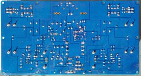
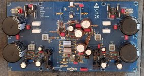
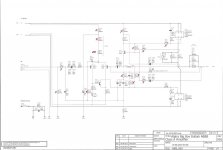
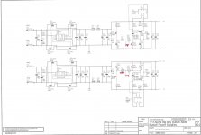
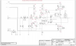
Attached are the schematics of the power supply and amp. Red "x"s denote blown resistors. The delay is not included since they are all blown.
Also attached are images of the top and bottom. I inspected the areas around the transistors with a magnifying glass before removal of the parts.
The power transistors and MOSFETs are wire-wound and soldered to the flying leads, so will require some surgery to check. When I built them, I gave every wire a good "pull test" to ensure the crimps are solid at the board end. I also verified I had closed circuits between each wire and it's nearest passive device.
Lastly, I double checked again that there is no short between the flying leads and the heat sinks.
The Chassis is made from wood, so nothing can short to the chassis.
My current plan is to replace all the resistors since most are blown anyway and are not terribly expensive. None of the polarized caps are mis-formed, so I expect they are good. I will also replace the three actives in the circuit protection area.
Any thoughts on the film caps or the on board transistors?
Again, thank you all very much,
-Josh
@AKSA I really appreciate the offer, and will gratefully take you up on it.
I will shortly send you an email with .zip file containing the uploads here at full resolution.
I re-checked all the wiring for the mosfets and power transistors, they are all correct.
I also compared the data sheets for all the active devices, and compared them to both the schematic and circuit board.
I checked as best as possible all the resistors. All the resistors in the delay are open, and a great number of them in the amp are open.
I removed several of the transistors to check them. All checked "fine" according to my $10.00 Chinesium component tester.
Checked transistors are:
V212 (Power supply NPN)
V111 (Amp NPN)
V321 & V322 (Circuit protection N MOSFETS)
Attached are the schematics of the power supply and amp. Red "x"s denote blown resistors. The delay is not included since they are all blown.
Also attached are images of the top and bottom. I inspected the areas around the transistors with a magnifying glass before removal of the parts.
The power transistors and MOSFETs are wire-wound and soldered to the flying leads, so will require some surgery to check. When I built them, I gave every wire a good "pull test" to ensure the crimps are solid at the board end. I also verified I had closed circuits between each wire and it's nearest passive device.
Lastly, I double checked again that there is no short between the flying leads and the heat sinks.
The Chassis is made from wood, so nothing can short to the chassis.
My current plan is to replace all the resistors since most are blown anyway and are not terribly expensive. None of the polarized caps are mis-formed, so I expect they are good. I will also replace the three actives in the circuit protection area.
Any thoughts on the film caps or the on board transistors?
Again, thank you all very much,
-Josh
Attachments
Hi Joshua,
That’s an awful lot of resistors to be blown. Even in places that don’t carry much current (like input stage). How are you measuring them? If you use a digital multimeter, are you sure your test leads are not bad or maybe the meter itself might be bad? There is no reason for R101 R102 to get blown - ever. In all my years of making amps, these are never damaged. Or you have a thin solder flux film over the terminals and the meter probe is not contacting the legs proper. You have quality Dale CMF55 there and they look fine. When they blow they will be brown or black and visibly burnt.
That’s an awful lot of resistors to be blown. Even in places that don’t carry much current (like input stage). How are you measuring them? If you use a digital multimeter, are you sure your test leads are not bad or maybe the meter itself might be bad? There is no reason for R101 R102 to get blown - ever. In all my years of making amps, these are never damaged. Or you have a thin solder flux film over the terminals and the meter probe is not contacting the legs proper. You have quality Dale CMF55 there and they look fine. When they blow they will be brown or black and visibly burnt.
Last edited:
Hi Joshua,
That’s an awful lot of resistors to be blown. Even in places that don’t carry much current (like input stage). How are you measuring them? If you use a digital multimeter, are you sure your test leads are not bad or maybe the meter itself might be bad? There is no reason for R101 R102 to get blown - ever. In all my years of making amps, these are never damaged. Or you have a thin solder flux film over the terminals and the meter probe is not contacting the legs proper. You have quality Dale CMF55 there and they look fine. When they blow they will be brown or black and visibly burnt.
I have an old Fluke 88 from my previous life, it's beat around a bit, but still works fine.
I double checked and found that you are indeed right, R101, and R102 are not blown. I should have caught this, a moments common sense says that if the amp is not hooked up to an output, then those should never blow.
I had the meter set to "alert", and did not realize that it stops auto-ranging....
Just goes to show that you can use a tool for decades, and still not know everything about it
I will upload a fresh schematic. I need to eat, and I am probably done for the evening, so probably tomorrow.
Thanks for the challenge on my info,
-Josh
Hi folks,
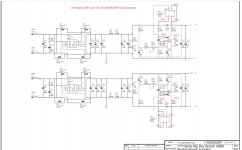
Here are some voltages.
I am running it at about 55VAC.
Attached are screen shots, and the original pdf with the values in red.
Should the base of V111 be 0V?
When I tried to measure R116 on the board, it acted like it was pumping up a cap, so I removed it and checks correctly.
Thank you all for your help,
-Josh
Attachments
Hi Joshua,
Thanks for posting the detailed diagnostics. There is something strange going on at the gate of the P-channel MOSFET and what is driving it - the KSC3503 VAS stage V104. The gate voltage should be about 4 to 5v higher than the -ve rail or -14v to -15v. For it to be at -0.25v or near 0v means that the MOSFET is either conducting wide open (smoking hot). This would explain fuses blowing, etc. I would remove the P-ch MOSFET and check the resistance between the gate and drain or gate and source and source and drain. If anything lower than 10's to 100's of kohms then it is probably a fried MOSFET (shorted between S and D) and G and D or S. It may have fried because the thermal conduction was not good, or ESD, or you may have a bad KSC3503. However, I find that the BJT has never gone bad in my experience.
Thanks for posting the detailed diagnostics. There is something strange going on at the gate of the P-channel MOSFET and what is driving it - the KSC3503 VAS stage V104. The gate voltage should be about 4 to 5v higher than the -ve rail or -14v to -15v. For it to be at -0.25v or near 0v means that the MOSFET is either conducting wide open (smoking hot). This would explain fuses blowing, etc. I would remove the P-ch MOSFET and check the resistance between the gate and drain or gate and source and source and drain. If anything lower than 10's to 100's of kohms then it is probably a fried MOSFET (shorted between S and D) and G and D or S. It may have fried because the thermal conduction was not good, or ESD, or you may have a bad KSC3503. However, I find that the BJT has never gone bad in my experience.
Hi Joshua,
Thanks for posting the detailed diagnostics. There is something strange going on at the gate of the P-channel MOSFET and what is driving it - the KSC3503 VAS stage V104. The gate voltage should be about 4 to 5v higher than the -ve rail or -14v to -15v. For it to be at -0.25v or near 0v means that the MOSFET is either conducting wide open (smoking hot). This would explain fuses blowing, etc. I would remove the P-ch MOSFET and check the resistance between the gate and drain or gate and source and source and drain. If anything lower than 10's to 100's of kohms then it is probably a fried MOSFET (shorted between S and D) and G and D or S. It may have fried because the thermal conduction was not good, or ESD, or you may have a bad KSC3503. However, I find that the BJT has never gone bad in my experience.
Thank you very much for taking the time to try and untangle this.
Sorry if it I was not clear in my previous post, all those voltages where taken with the MOSFETs disconnected. I put it on the schematic, but I think I forget to say that in my post.
The P-MOS checked fine by your suggestion, the N-MOS though was shorted by all pin combinations.
I have replaced the N-MOS, and started the amp.
There is a hum coming from something. I do not know what, it might be the fans, might be the variac, the toroid, something else...
Voltage drop over the source resistors climbs up to about 0.7V and then settles at 0.64V.
I slowly raised the variac, source resistor drop remained constant, and the hum seemed to get quieter.
At about 100V, the C-60 started to smoke and I shut it off in a hurry.
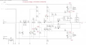
Attached are voltages using about 70VAC. This is enough AC to get the fans running and the temp display working. Temp stays under 60C measured on the heatsink die with thermistors.
All voltage are with MOSFETs connected
Note the "?" at the base for V111. Probing this changes the pitch of the hum, and the display changes intensity.
Thanks again.
-Josh
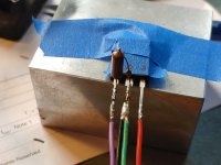
I also attached a pic of the wires at the N-MOS for those interested in that sort of thing
Attachments
Well, I got the amp running.
Turns out the root cause was torque from the wires causing the transistors put too much pressure on the Silpads allowing them to partly short when at near full power. I happened to be looking in the right place at the right time, and saw a bit of blue glow.
Yes, I do polish off any burs before mounting transistors.
Now I am having a loud humming from my speakers (both amps).
I only get the hum when connected to my DAC or AVR.
I do not get the hum when I use the headphone jack from my phone or when the audio in is disconnected.
Here is what I have done so far:
Detached the audio in from the back panel.
Run "jumper" binding posts directly from the circuit board to bypass the installed binding posts.
Detached the safety ground from the heat sinks.
Unplugged the transformer from the bridge rectifier that runs the fan controller.
The chassis is made form wood.
The ground scheme as of this moment is mains earth goes to the star ground, the back panel safety earth and the clean ground from the amp go to the star ground.
Power comes in, goes to a distribution block, to the transformer, to the amp. The 12v tap is detached from the rectifier.
There is a class X/Y cap across the line and neutral.
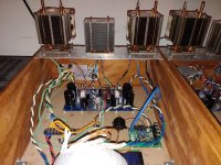
Attached is a pic of the inside. I can take a decent pic of any area anyone wants to see.
I do have one question in particular, is it safe to float the ground on this amp?
Any ideas or suggestions greatly appreciated.
Thanks,
-Josh
Turns out the root cause was torque from the wires causing the transistors put too much pressure on the Silpads allowing them to partly short when at near full power. I happened to be looking in the right place at the right time, and saw a bit of blue glow.
Yes, I do polish off any burs before mounting transistors.
Now I am having a loud humming from my speakers (both amps).
I only get the hum when connected to my DAC or AVR.
I do not get the hum when I use the headphone jack from my phone or when the audio in is disconnected.
Here is what I have done so far:
Detached the audio in from the back panel.
Run "jumper" binding posts directly from the circuit board to bypass the installed binding posts.
Detached the safety ground from the heat sinks.
Unplugged the transformer from the bridge rectifier that runs the fan controller.
The chassis is made form wood.
The ground scheme as of this moment is mains earth goes to the star ground, the back panel safety earth and the clean ground from the amp go to the star ground.
Power comes in, goes to a distribution block, to the transformer, to the amp. The 12v tap is detached from the rectifier.
There is a class X/Y cap across the line and neutral.
Attached is a pic of the inside. I can take a decent pic of any area anyone wants to see.
I do have one question in particular, is it safe to float the ground on this amp?
Any ideas or suggestions greatly appreciated.
Thanks,
-Josh
Attachments
Grounding scheme is hard to see from photo. Can you make a hand sketch of the grounding plan?
What is important is that the clean analog ground of your amp doesn’t touch the dirty chassis ground directly or inadvertently. It must be controlled and deliberate.
For example, here is what I did for the Alpha Nirvana amp:
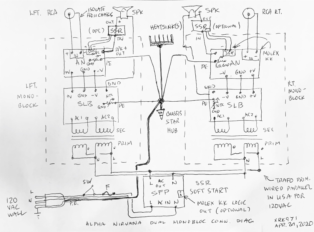
What is important is that the clean analog ground of your amp doesn’t touch the dirty chassis ground directly or inadvertently. It must be controlled and deliberate.
For example, here is what I did for the Alpha Nirvana amp:
Thanks for the reply.
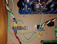
Here is a sketch of the grounding and powering scheme, and a pic of the actual implementation.
Everything in the power/ground path is in the sketch - if it is not in the sketch, it is not in the amp.
A note: the ABBB has a C-60 at the ground on the circuit board, so I am not further isolating the ABBB ground with another C-60.
Should I still have another C-60?
The disconnected green wire is the safety ground to the heat sinks.
The tightly wound black and white wires crossing the circuit board that appear to touching the transistor are not touching the transistor. it is an optical illusion, the wires and the transistor are several inches apart.
My line power is reasonably clean. I take pains to not use fluorescent or LCD lights, and I do my best to keep SMPS's off this circuit.
The humming sound is similar to the humming sound you get when you plug a guitar into a live amp. About that same frequency, but not as loud and without the "buzzing."
Thanks again for your help,
-Josh
Attachments
- Home
- Group Buys
- The Alpha Big Boy with Buttah (ABBB) 52w Class A Amp GB