I think it is possible by changing bulk caps to 10,000uF 63v. And make sure all the electrolytics downstream are rated appropriately. You will need to feed it with circa +/-53v under load to account for 3v drop through the cap Mx, and assume about 4v sag so under no load needs to be =/-57V. 57v x 3A x 2 rails = 342W dissipation, to give headroom, size trafo to be at least 2x more than dissipation, so a 40Vac 600VA trafo should do it. For example Antek AN-6440.
Last edited:

View attachment SLB v1.2 Schematic May3.pdf
Hi X,
In the wiring diagram you published (attached #1), you show an 8D-20 NTC thermistor in series with the power traffo primary.
These are 8 ohm 6a devices.
Can you please tell me:
1. Is this the same as 'TH1' specified in the TLB schematic (attached #2)?
Or are both needed?
2. TH1 - as specified in the Mouser 'project' is an 8D2-07LD ... which is an 8 ohm 2a device.
Is there any reason not to use an 8D-20 here, instead?
Thanks,
Andy
Just use 8D-20 if you have them. I get them in bags of 20 so have lots to use.
That's what I was hoping, X - seeing as you have to buy 20!
")
But can you tell me whether using an 8D-20 NTC thermistor in series with the power traffo primary means you don't need 'TH1' ... or do you need both.
Andy
You need both, the onboard TH1 is for the chassis return ground loop breaker.
If you happen to have a CL60 on hand, use it there it’s slightly smaller. That gives a little bit more room for my fat fingers to attach faston connectors
Thanks, Vunce.
Andy
It's definitely not something you want to grab with your fingers when it is running, but doesn't melt its own solder at least and we are giving it room for air flow. If folks are concerned about keeping temps low, use four 0.22R in series parallel and dissipation will be about 1.25W each for maybe 65C temps.
Mr. pass in general uses four 0.47 res in paralel. Is there any particular reason to use two 0.1 ohm in series?
And in the above suggestion four 0.22 in paralel is not equal to two 0.1 in series i guess?
Thanks
Because we wanted 0.2ohms and 10w (with two KOA Speer 5W BPR's), not 0.12ohms and 12w (4x Panasonic ERX 3W). It's not the same CRC as a standard CRC alone PSU. This CRC and cap multiplier were simulated in LTSpice to minimize ripple upstream of the cap Mx while making sure that the ripple current is not exceeded.
Because we wanted 0.2ohms and 10w (with two KOA Speer 5W BPR's), not 0.12ohms and 12w (4x Panasonic ERX 3W). It's not the same CRC as a standard CRC alone PSU. This CRC and cap multiplier were simulated in LTSpice to minimize ripple upstream of the cap Mx while making sure that the ripple current is not exceeded.
I see thanks then WSR5R1000FEA could be a good candidate but i can not find its surface temp vs watt graphic.
Jhofland did the simulation on the CRC part and Aksa did the simulation on the CFP cap multiplier separately, so not in one simulation. It's not a hard circuit to replicate yourself, no exotic parts were used. Just apply 50/60Hz AC ripple upstream of the CRC and see what it is dowstream. Monitor the rms AC current a.k.a. the ripple current during the charging and discharging cycles of the caps and make sure it doesn't exceed the rated value for the cap.
The circuit has been optimized, especially the cap multiplier part. I would mot change that side much., it can go unstable if not done right. A more foregiving topology would be a Darlington based cap multiplier.
The circuit has been optimized, especially the cap multiplier part. I would mot change that side much., it can go unstable if not done right. A more foregiving topology would be a Darlington based cap multiplier.
Note that even a cheap stamped aluminum serated style fin heat sink works fine. It’s not a lot of heat so big Aavid’s are not critical. Look at my build photo to see what I did.
The big Aavids look nice though - if you really want those - get them.
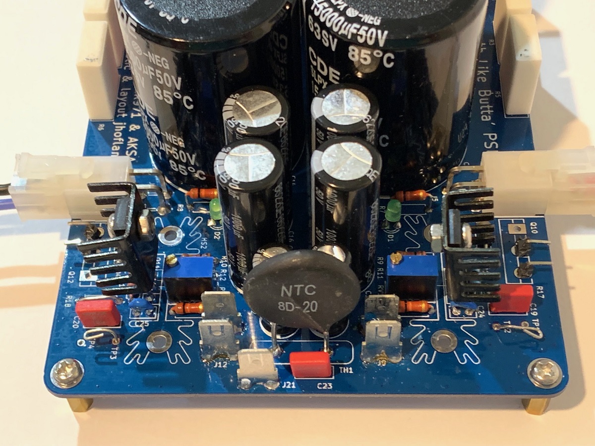
X - can you tell me what the strange bent pieces of wire are for (which are adjacent to C19 & C20)?
Thanks,
Andy
X - can you tell me what the strange bent pieces of wire are for (which are adjacent to C19 & C20)?
Thanks,
Andy
They look to be test points (TP). Wire soldered in to attach a test clip to.
They look to be test points (TP). Wire soldered in to attach a test clip to.
Of course - thanks (yes that makes sense).
What are they testing, though?Examining one of my SLB boards, though, I see there's:
* 'TP1' and 'TP2' on the 'P' side, and
* 'TP3 and 'TP4' on the 'N' side.
So I'm wondering why there aren't similar wires soldered into TP1 and TP4? What are they testing?
Andy
Last edited:
They are labeled with silkscreen - just refer to the schematic:
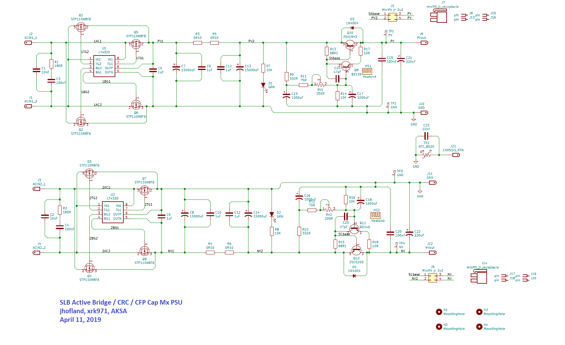
TP1 and TP4 are connected to the output voltages, same as BJT collector pins.
If you look carefully, you can see I added test points to the BJT collector and emitter. Those let me test upstream vs downstream voltage.
TP1 and TP4 are connected to the output voltages, same as BJT collector pins.
If you look carefully, you can see I added test points to the BJT collector and emitter. Those let me test upstream vs downstream voltage.
They are labeled with silkscreen - just refer to the schematic:
TP1 and TP4 are connected to the output voltages, same as BJT collector pins.
If you look carefully, you can see I added test points to the BJT collector and emitter. Those let me test upstream vs downstream voltage.
Thanks, X.
Yes, I now see:
* TP1 is connected to Q10 collector
* TP4 is connected to Q12 collector
* and Q2/Q3 are connected to Ground.
But looking at the emitter side of these output BJTs ... I can't see any more TPs?
Andy
That’s what the test points on the spare BJT pads was for. I agree a proper test point could have been made and maybe there is one on the production board. But you just need to be clever and look around for an exposed lead somewhere.
Thanks, X.
Now, I have a Qu about the SLB for the AN 4R version.
In the standard SLB (for the AN 8R), R7, R8 and R14, R16 are 10K - and the DC rails are at +/-27v.
Does this value need to be reduced for the AN 4R - given the DC rails are +/-20v? To, say, 8K?
Andy
- Home
- Group Buys
- The SLB (Smooth Like Butter) Active Rect/CRC/Cap Mx Class A Power Supply GB