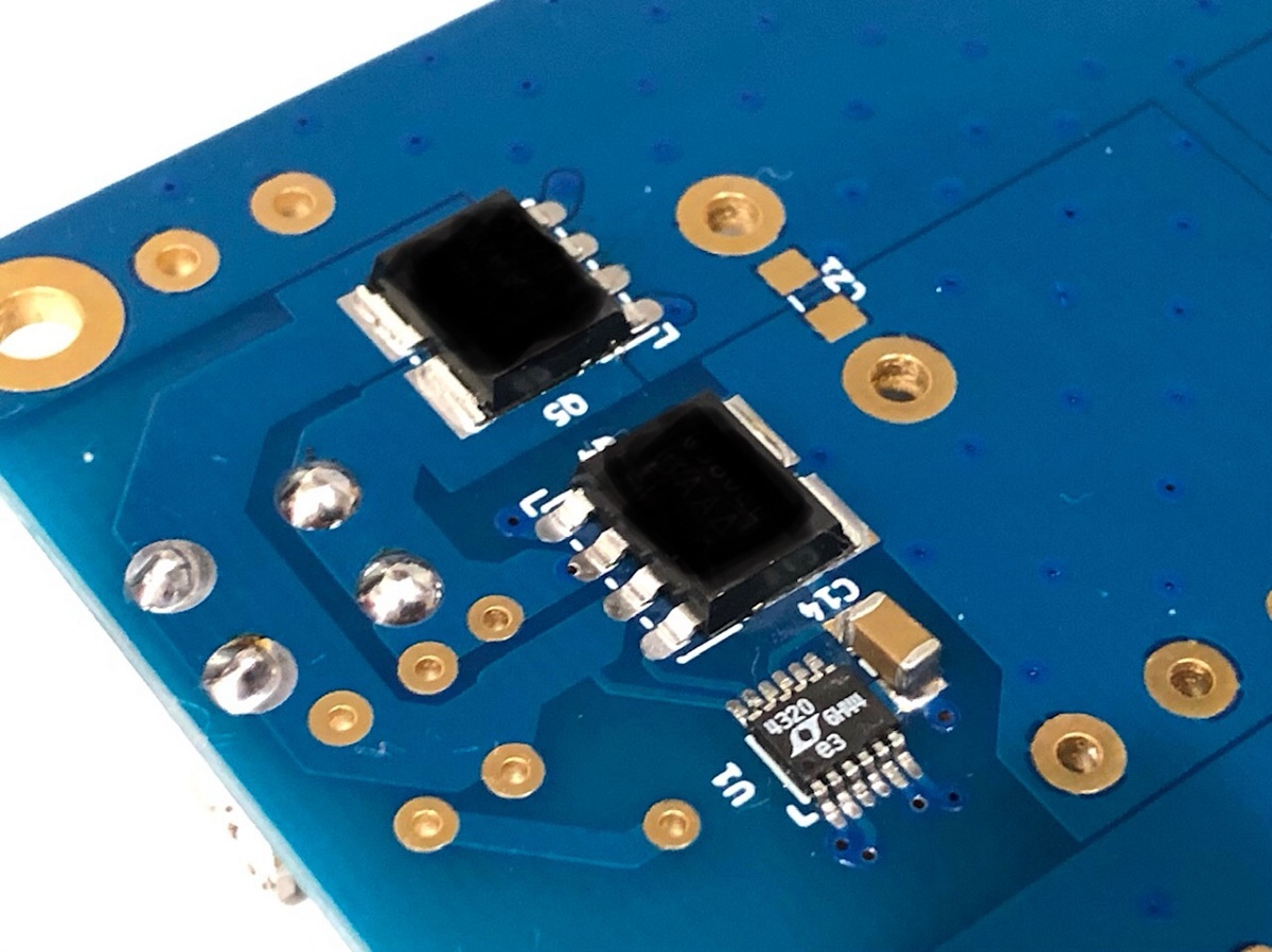
The paths of the SMT prototypes were indeed tight and small. Jhofland did a great job on keeping the design tight to minimize the loop current area. Here is a closeup of the SMT active bridge. It doesn't get much tighter than this:
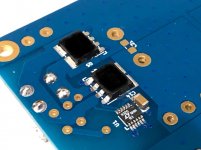
For the SLB, we wanted to make it accessible to the average DIY'er who doesn't want to do SMT soldering. So compromises had to be made with using four TO220 MOSFETs, spacing is larger, DIP 8 version of LT4320, etc. But I think it should be all good. I will order a set of verification boards and test to make sure there are no extraneous switch noises or oscillations etc before releasing the final (verified to be working) board for the GB. This extra level of work and due-diligence is what gives the DIYA community the peace of mind that they won't be getting a dud. It's a lot of extra $ and work but worth it in the end.
For the SLB, we wanted to make it accessible to the average DIY'er who doesn't want to do SMT soldering. So compromises had to be made with using four TO220 MOSFETs, spacing is larger, DIP 8 version of LT4320, etc. But I think it should be all good. I will order a set of verification boards and test to make sure there are no extraneous switch noises or oscillations etc before releasing the final (verified to be working) board for the GB. This extra level of work and due-diligence is what gives the DIYA community the peace of mind that they won't be getting a dud. It's a lot of extra $ and work but worth it in the end.
Attachments
Last edited:
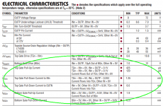
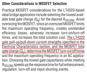
The LT4320 datasheet gives customers all the data they need, to calculate turn on and turn off time. The MOSFET gate drivers, which are output pins on the LT4320, have a Thevenin equivalent circuit that is definitely not an ideal voltage source. External resistors in series with the MOSFET gates would be superfluous.
And, if it so happens that Linear Technology offers an LTSPICE model of the LT4320 (?), I expect their model gets this important detail exactly right. Pair it with a MOSFET spice model that actually does simulate Qgtot = 150 nC, and you get an acceptably accurate simulation of turn on and turn off. Plot the current waveforms and look for fast transients / high frequency components if you worry about those. Plot MOSFET power dissipation if, like me, you are concerned about that.
_
Attachments

Mark is right, certainly not a power house of a driver. So there will not be much EMI from the gate drive which is good news. But a quick test in LTspice with a 140nC FET shows it a bad idea, it cannot drive the gate more than 4-5V, and at that gate voltage the Rds-ON is not as low as it can be. Might as well use FETs that have lower Qg so they will be driven properly and you get low enough Rds-ON.
I think when selecting FETs you want low enough Rds-ON, not unecessary low. That way you select for each load. One load may draw 1A, another 5A etc. Dont use same beefy device on both.
I think when selecting FETs you want low enough Rds-ON, not unecessary low. That way you select for each load. One load may draw 1A, another 5A etc. Dont use same beefy device on both.
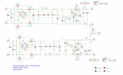
We have revised the schematic to include a 47pF capacitor between the collector and base of the master BJT and a 10R resistor between the emitter of the master BJT and the output. This will give us an opportunity to squash any oscillations, should they arise. Board layout outline size remains the same size. Parts list (BOM) is also attached below.

Attachments
Last edited:
Our simulations show that the CFP topology should be even better.
You probably want to run them again, including the two new components in the CFP output stage. You've cut its effective gm = dI/dV by about a factor of 5x, and I imagine there is a very real possibility this will impact your measures-of-goodness. The ways you quantify "even better" in the quote above.
The response to a square wave of output current will be affected, to name one example. Whether the difference is small enough to be disregarded, is a human decision.
You might not get a great deal of Miller Effect from the new 47pF capacitor, since it's effectively voltage driven rather than current driven. Open loop simulations with, and without, that capacitor will tell you how much it does or does not help.
_
Attachments
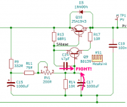
The idea was to have those positions available in case we see oscillation - but will initially leave unpopulated. As I said, our earlier tests with the CFP cap Mx had issues with oscillation. We will redo the simulation though to make sure performance is not too negatively impacted.
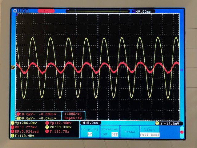
Some more data running a real amp as load. This time with is oscope ch1 on output of cap Mx and Ch2 on input to cap Mx (after active bridge and CRC). For 4.35A and 27.5v to the amp. Getting 99mV rms ripple which looks almost sine wave like, and 3.3mV rms downstream of the cap Mx. This is the Darlington variant.
Attachments
Last edited:
One PCB is dual rail and can provide up to 5A continuous current. Depending on your rail voltage, may be enough for much more than a 25w amp. I use just single rail at 37v and 4.35A for a 50w SE Class A amp.
For the typical +/-24v At 1.25amp PSU needed for 25w Class A amps out there, this supply will not even break a sweat. For lowest noise and to minimize chances for ground loop hum noise, I highly recommend one dual rail per trafo per channel for monoblock operation. Having left and right channels share a common PSU often results in ground loop hum.
For the typical +/-24v At 1.25amp PSU needed for 25w Class A amps out there, this supply will not even break a sweat. For lowest noise and to minimize chances for ground loop hum noise, I highly recommend one dual rail per trafo per channel for monoblock operation. Having left and right channels share a common PSU often results in ground loop hum.
Jhofland and I have had numerous discussions around the subject of where to put the R in a CRC. I normally split them with one across the positive and one across negative terminals. The sims show that it makes no difference where they are placed as the return current has to form a loop.
Another question X, for the usual +/- 24VDC supply to feed the power amp from the output of this design, what is your recommended transformer secondary voltage feeding the board?
I also assume that the transformer must have dual secondary windings and not a centre tapped winding?
Do you think there would be any added advantage in slotting in a separate CRC or CLC board between the output of this board and the power amp for extra supply stiffness.
For the schematic you have shown, what is the equivalent total capacitance the amp would see using the cap multiplier as shown on the PCB?
The cap multiplier really is a ripple eater so comparison of equivalent “capacitance” is not of real value since real capacitors provide a storage of energy, whereas the cap Mx or ripple eater acts as if it is a very large C in a CRC filter but has no storage of energy. You could calculate what the equivalent C would be needed to give a 3.6mV ripple for 37.5v at 4.35A. It would be pretty big. So capacitance multipliers really are suited for Class A amps where the current is steady. So “stiffness” isn’t needed and doesn’t really apply like it would in a Class AB amp where the current is changing with the music.
This supply is all you need, no more CLC or CRC needed in addition. When used with my SE Class A amp, it is so quiet I can’t tell the amp is even turned on with my ear pressed to the speaker cone.
How to size the trafo? Depends on the brand a bit. I would size the VA rating at 3x nominal requirement to reduce sag and saturation. So for +/-24v at 1.25A that’s 48v x 1.25A that’s about 200VA and voltage at required rails plus 3v for the cap Mx and probably 4-5v more for sag. So 24v +3v + 4v = 31v. Now divide by 1.4 and you get 22v. So for the typical 25w Class A amp, use dual 200VA 22v trafos one per channel. Note that some brands like Antek sag more than others so step up one more notch to 24v. But maybe a Talema or Toroidy is fine at 22V. Yes, dual secondaries not center tapped. One more thing, it never hurts to go up one more notch in VA rating either so dual 300VA would assure you of even better performance.
Last edited:
SLB Group Buy List
baswamin - 2 boards
meanie - 2 boards
jwjarch - 2 boards
gary s - 2 boards
Total = 8 boards.
Looking forward to using these to mate with your Alpha 20 PCB's received recently, which I will build as dual mono designs. Very interested to see how they will compare to the MX2.
Any anticipated pricing yet or when they will be available?
However it does prevent at least one type of disastrous PCB layout.Jhofland and I have had numerous discussions around the subject of where to put the R in a CRC. I normally split them with one across the positive and one across negative terminals. The sims show that it makes no difference where they are placed as the return current has to form a loop.
I am about to order a set of verification pcbs. Will build it and verify that it all works. Then order final set. So probably 3wks away at least. Boards will be 2mm thick, 2oz copper, ENIG finish and blue solder mask. Probably about $23ea. Usual shipping charges of $5 in US, $10 in CAN and $15 everywhere else. I am not sure how heavy they will be, so above shipping is approximate and might be a little more.
where to put the R in the CRC
Putting them in the low side and the high side does have a practical problem, at least for the layouts I do. The resistors themselves dissipate enough power to get pretty toasty. So you want to place them where they can get some reasonable air flow. Those in the low side tend to get trapped between the large filter caps which restricts cooling somewhat and the added space between the caps increases board area and ripple current loop area.
However it does prevent at least one type of disastrous PCB layout.
Putting them in the low side and the high side does have a practical problem, at least for the layouts I do. The resistors themselves dissipate enough power to get pretty toasty. So you want to place them where they can get some reasonable air flow. Those in the low side tend to get trapped between the large filter caps which restricts cooling somewhat and the added space between the caps increases board area and ripple current loop area.
- Home
- Group Buys
- The SLB (Smooth Like Butter) Active Rect/CRC/Cap Mx Class A Power Supply GB