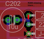
Found one little trace missing, was probably lost when I rearranged the pcb for the J113. It is between R209 and R208/C202. Simply solder a small piece of resistor leg or there won't be any signal at the 'Right' output terminal. Found no other error... See the image.
SB
SB
Attachments
Here the measurements I did, take note that the gain and THD content depends on the tube bias adjustment pot...
Gain: 17.8dB (Vin: 200mV, Vout: 1.545V, max volume) Note: B1 JFET stage are just buffer, gain of 1, the gain comes from the Nutube only...
Vin max: about 0.8Vac, 1Khz (max volume)
BW: 52Khz (Ref 1Khz, 1Vout)
Noise: 0.06mVac (shorted input)
THD, depends on tube bias pot, can be almost null out, up to very high values...
Tested with source 1Khz, 0.006% THD, Vout 1V, can be adjusted down to 0.09%
Supply ripple, at ''F'' point = 0.04mv, at ''R'' point = 0.03mv (the supply ripple is extremely low...)
So it is working perfectly. Tomorrow I'll try to mount the pcb into the enclosure...
Last edited:
PCB had been working overnight non stop without problem. I would suggest that you lift from the pcb the 3W power resistors, in particular the 270R. It is cooking a little, nothing serious 0.6W into a 3W resistor, but installed it a few mm from the PCB will improve the heat transfer.
Not assembled into an enclosure yet, and no RCA in stock ")
Will mount everything and I'll have a listen in a few days.
It is comming, don't worry
I put together a little document that resume the PCB corrections. It will be sent with the latest documentation revision to all GB members after they do the last payment for the shipping cost.
The documentation includes a detailled schematic with a lot of reference voltage readings, to help you test your circuit...
Thanks
SB
Last edited:
Some asked for an assembly guide. I was planning to do one, but here a quick starter:
Hi. Not really, but I can help you with a quick guide:
SUPPLY________________________________
1) First solder the smaller smd parts near the SMPS module, starting with the larger smd cap C3, then the inductor L1, then C1 and C2. Check there is no short between V+ and V- pins of the SMPS module
2) install the AC side parts before the SMPS module. Make sure to use a fuse for testing. I used 1A FB...
3) Install the SMPS module, plug the pcb into AC line and insure there is a stable +24V at the 24V/GND TP, mine read 23.92V. Disconnect AC and let discharge the caps. Note: If you don't want to use the builtin SPMS power supply, you can still use an external 24V supply, in this case connect it to the 24V/GND Test point...
4) Install the 3W resistors, slightly elevated from the PCB.
5) Install the rest of the supply section, C4-C10 and both 9.1V zener
6) Re-connect to AC line, insure there is about 24V at ''F'' test point (just over the tube), and +9V at the zener cathode.
PREAMPS SECTION____________________________
7) For the preamp section, solder all the resistors and trimmers.
NOTE: Rled, value not specified because it depends on the led used (color) and the intensity you want. Can be from a few Kohms to up to 30-47K if using a blue led, test it and select accordingly...
8) Solder remaining caps. Take care around C203, incorrect silkscreen. Also add the small missing link between R203 and R208, see PCB correction doc.
9) Connect supply again, and make sure the supply is still ok, and there is no short, disconnect supply and let discharge...
10) Install the K170GR JFET. They need to be match 4-5ma IDSS by pairs, ideally the same IDSS range for all JFET... The J113 need a resistor, J-R1 on the PCB. I haven't tried the J113 option, so can't help you there...
Install ONLY the K170 OR the J113, not both at the same time...
11) Once the JFET are in place, power-on and check the various DC voltages according to the schematic I sent you. The first section of the buffer (Input Q100/101, Q200/201) works fine without the Nutube installed. The stage after the Nutube needs the tube to complete the circuit, but you can still insure there are voltages and no short...
12) Let the supply discharge, and finally install the Nutube. Check voltages according to the schematic. Volatges around the Nutube depends on the trimmer setting, see below. The tube Gain and THD and bias point depend on the trimmer adjustment. You need at least a scope to get the best adjustement (nicer output waveform), and really some THD analyzer (sound card, etc) to be able to null out the best THD level...
Also there is a possibility that both sides of the tube are not exactly the same, so you can probably expect some difference between channel volt readings
Take note that the JFET Buffer sections, have no gain (Gain of about 1), and that the gain comes from the Nutube.
13) If everything is ok with the preamp circuit, you can mount it into an enclosure, connect the input selection switch, and the option of two separate single volume pot, or one dual pot. Keep in mind that you can have a slight difference in gain between each channel, so the option of the two single volume pot can be use to compensate for that. You can always compensate for the difference in gain with the trimmer, to some extend...
Note: the inputs pads were designed to accomodate small PCB Turret, Harwin (Mouser 855-H2121-01) or simply solder your wire.
These turrets insure strong, reliable wire connection, that you can unsolder countless time without damaging the PCB.
If you want to use the turret, as I did, you can install them like that:
1) Install the turrer upside down into a small vise,
2) place the PCB over the turret end, then
3) using a small punch and hammer, and (gently...) punch the turret end in place, repeat until you have a strong connection.
4) repeat for the other location. BTW these turrets can also be installed on the 24V/GND TP location
5) for better result solder the turret from top and bottom.
14) Install the In/out connector, front power-on led and pots, and make a final check.
I did a very detailled schematic with reference voltages everywhere. It is your primary tool to check/test the pcb. Please don't forget to have a look at it
ASSEMBLY COMPLETED...
Last edited:
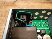
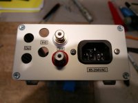
And I should add to connect the AC inlet ground connection to the frame, see first picture, at least in North America.
Safety ground may be different in you country...
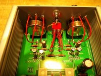
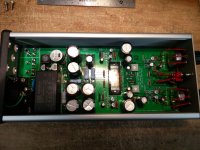
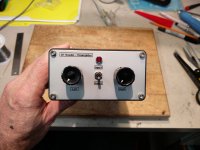
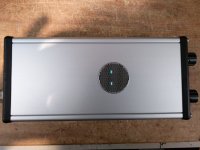
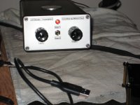
To complete my little assembly guide, here picture of my won preamp, missing a few RCA connectors on the back, but you get the idea
Check my little ventilation window on top, we can see the tube looking at you
BTW I used a 22K resistor for Rled, with a red led...
SB
Safety ground may be different in you country...
To complete my little assembly guide, here picture of my won preamp, missing a few RCA connectors on the back, but you get the idea
Check my little ventilation window on top, we can see the tube looking at you
BTW I used a 22K resistor for Rled, with a red led...
SB
Attachments
It is from a Polaroid ultrasonic range sensor (from the 80's), now used with robots, see: Ultrasonic Sensors, Piezoelectric Ultrasonic Sensors | SensComp
I got mine from a defective one. I have my own little stach of it
I got mine from a defective one. I have my own little stach of it
Last edited:
Attachments
- Home
- Group Buys
- GB B1 Nutube PCB with integrated PS