HiWhat was the procedure for obtaining the full manual again? The project has been on an unfortunate hold for me for a while but I’m getting back on it! I do have all the components and I’m finishing the power supplys at the moment.
Sorry I have not received an automated notification about your message. I just sent you the full build manual of USSA-5.
Fab
Last edited:
Fantastic, thanks Fab!Hi
Sorry I have not received an automated notification about your message. I just sent you the full build manual of USSA-5.
Fab
I think I'm a bit overvoltage with my power supply. I'm getting 35V. This is just measuring from the power supply itself, so adding a load will drop that voltage somewhat, but I will still be in the 32V ballpark, perhaps slightly over. Am I OK if I make sure I have enough heatsink, or should I take other measures?
Hi Nikodemuzz
The load would be the bias current. if you have enough heatsink capacity that still would be ok but that depends how much power in class A you want.…Also, have in mind that the J112 fet are 35VDC max. To be in the safe side you can increase R11/12 from 10 to 1K ohms but in the manual just change 28mV to 2,8V For the measurement of input stage current.
The increased power supply voltage will also increase the power in the transistors but should normally be still ok. However, I recommend that you monitor closely the output transistors current via R15/16 so it stays in control. If it tends to always increase over time you may have to reduce the value of R7/8 by 20% or so for example. You would need to experiment. This is especially true for the bjt output version. The lateral mosfet version should not be much impacted.
Good luck
Fab
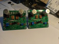
Do you ship to india. What would be the cost for shipping to indiaPicture of bare pcb
Pcb picture
98mm x 84mm
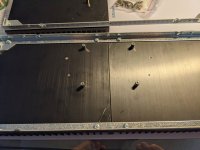
Good progress.USSA 3.0 in the making!
Glad to know that you build version 3.0 since this one is more rare since matched input jfet cost an arm and mosfet drivers have been obsolete since a long time.… normally you should get a big soundstage
")
some observations or reminders:
1) potentiometer screw relative position when installed on pcb determines the resistor value direction change. In one board one for the 2 bias/dc offset pots it could be more « difficult« or not a consistent way to provide adjustment between left and right channels…
2) RV1/2 are mandatory to ensure right connection. Either use the calculated resistor value or a wire link.
good luck for the rest
Fab
Last edited:
The k2013/j313 costed me more than the jfets.
And buying only 2 pairs of Exicons at Profusion is not cheap either!
Spotted the bad trimpot orientation but thought that with my skills, it'll be cleaner to adjust in opposite direction than desoldering it properly...
I have to read again the RVxx thing.
And buying only 2 pairs of Exicons at Profusion is not cheap either!
Spotted the bad trimpot orientation but thought that with my skills, it'll be cleaner to adjust in opposite direction than desoldering it properly...
I have to read again the RVxx thing.
Regarding the jfets, did you manage to find matched GR grades, or LSKxxA pairs? I can only find matched BL or LSKxxB pairs.The k2013/j313 costed me more than the jfets.
yes I saw the store offer. Those are BL/B grades, good enough to meet requirements but resulting in a lower DF than GR/A grades.Buy from the store, all you need is Idss below 8 mA, thanks to Papa, it's easy!
For jfet IDSS grade I have specifield <=8 ma which is on the low side of the BL grade. Damping factor value is slightly changed but not drastically-at least sound wise. In fact, DF value is more a personal preferenc in the end and also in relation to the rest of your system. The few USSA3.0 amps that have been built were using jfet BL grade IDSS - for the ones that I am aware of.
Tin any case the DF value will not be that high but surely high enough to not be a concern - like maybe some tube amps with very low DF. High DF (> 100 or more) has no real purpose - and even sometimes could sound « thin »(all other things being equal).
So either GR or BL it should sound like an USSA 3.0.
Fab
Last edited:

Hi Nikodemuzz
good progress too!
you really should adjust the current sources before installing the mosfet drivers. The current sources jfet can have very different IDSS resulting in a very unbalanced current between positive and negative sides of circuit. This could potentially damage your drivers or output transistors (too high power dissipation) before you can even adjust the current properly. I have indicated to use a lower power supply voltage in that part of the build manual only because I thought a bench power supply was available to use instead of the real amplifier power supply - which also may not be validated.
USSA 3.0 does not need current sources since it uses input stage jfet self biasing property and the jfet are matched.
The test parts are the most interesting feature of the build manual to validate at different steps of the assembly to avoid frustration in destroying expensive parts….
Therefore , please adjust the current sources first…
and then test with the drivers and then afterwards test with output transistors- as per the manual. Then you can be a happy monkey🐵
good luck
Fab
Last edited:
Thanks for chiming in Fab!Hi Nikodemuzz
good progress too!
you really should adjust the current sources before installing the mosfet drivers. The current sources jfet can have very different IDSS resulting in a very unbalanced current between positive and negative sides of circuit. This could potentially damage your drivers or output transistors (too high power dissipation) before you can even adjust the current properly. I have indicated to use a lower power supply voltage in that part of the build manual only because I thought a bench power supply was available to use instead of the real amplifier power supply - which also may not be validated.
USSA 3.0 does not need current sources since it uses input stage jfet self biasing property and the jfet are matched.
The test parts are the most interesting feature of the build manual to validate at different steps of the assembly to avoid frustration in destroying expensive parts….
Therefore , please adjust the current sources first…
and then test with the drivers and then afterwards test with output transistors- as per the manual. Then you can be a happy monkey🐵
good luck
Fab
Hmm, now I'm slightly confused. By mosfet drivers you mean the Exicons? M1 and M2 in the BOM? I don't think I'm supposed to touch those until way later in the process, and I haven't. I have tried to follow the manual to the letter. Besides resistors, I have installed only the D1-4, J1-4, Q1-4 and the potentiometers.
Maybe I caused the confusion by stating that I will build first and measure later. I was referring to our earlier discussion and potentially changing some of the resistor values to accommodate the slightly higher voltage. I meant that I would complete the build and observe if there is enough voltage drop "naturally" to not need any changes.
My intention was very much to proceed with the build according to the manual, with the next step being current source adjustment. =)
Hi @ntfsgame. Any further update… ? CheersHey guys, I'm in Italy till next monday evening for work. I hope I can finish the package after my return.
Just checking in again... maybe if it's not available then a 50w version of USSA might be possible given adequate cooling?Hi @ntfsgame. Any further update… ? Cheers
- Home
- Group Buys
- USSA-5 PCB GB