I ended up having 2x2 pairs matched at about 27mA+-0.2mA. Got everything build, and see a DC offset of 25mV on left channel, which is OK-ish, but the right channel has an offset of -0.48V. Negative MOSFET is draining more current than the positive one. Voltage across R138 is 340mA and 300mA across R137, both are 2R7.
I'm not sure why that is the case. I have measured all resistors before soldering (obviously JFETs as well), inspected every joint many times, but the offset is there.
R126 is definitely OK, so the suspect is R128, but I have measured it before soldering, so why would it cause problems? R128 is actually through hole, so I don't want to take it out just yet. I have made an experiment of putting another resistor across R128 and it actual "worked". I mean that it eliminated the offset. I had to put some 400ohm across R128 which indicates that its 330ohm. It's really hard to believe. What other possibilities shall I check?
Last edited:
Hi PiotrL,
Please check with DVM probe all the voltages at each node of all actives and write by hand into the schematic. Then take photo or scan and post here. That’s the only way we can debug - it’s like a blood test and X-ray in an ER her they want to find what’s wrong with a person’s health. The major nodes are every leg of an active, the output node, and bias current in all legs.
My guess is you have a part that is incorrect or a cold solder joint. Take an iron and touch ea h joint to remelt it.
Parts variation can’t mKe 480mV offset. So it has to be a bad or incorrect part. Do you have correct sex BJT in place? Are all MOSFETs P-channel?
For convenience, here is schematic:
https://www.diyaudio.com/forums/att...-class-hpa-sub-ppm-thd-shpa-sch_001_page1-pdf
Thanks Xrk. All parts are sourced directly from links in the excel ss (Mouser). I did not measure BC857s, however having two spare left, they look ok on DCA75.

So I though that melting each joint will be easy first step. It was easy, but made things worst, output DC offset is now -0.75V.
So I though that melting each joint will be easy first step. It was easy, but made things worst, output DC offset is now -0.75V.
OK, so I pulled out V124, but it measured fine on DCA75 and identical on Idss. This is actually impressive considering what it went through. I have done the same to V131 just in case because I did not measure it before and because it also differed from left channel equivalent . It was also OK. Next I checked all resistors around them, again OK. At this point I started to think that the circuit actually works fine, and it does what it supposed to do. It's just that there is something else on the board that pulls Vs of V124 down to 0.78V from about 1.5V like it is the case on the other channel.
I put back V124 and V131 on the board powered it up and observed same DC offset of -0.75V. Good: same predicateble behavior. So I stopped looking for faulty components and started looking for "additional/unwanted ones". I started scrubbing the board from flux dirt and started to remove excess of solder specifically around places where there are ground plane vias very close to component pads, and bingo! DC offset on the right channel in now -65mV, still high but R128 is actually not very well matched to R126 - this will get addressed later.
I have measured all voltages again FYI and indicated those which were wrong but now are matching left channel quite well. I'm sourcing this amp now from Arcam Irdac and listening to it on MSR7s. It eats my ifi iDSD nano for breakfast. Really impressive. All that bloody SMD work was a price worth paying for what I'm hearing now")
Thanks again for help. I'll be back when I'll sort all remaining bits and pieces out and have a finished product in a decent case.


I put back V124 and V131 on the board powered it up and observed same DC offset of -0.75V. Good: same predicateble behavior. So I stopped looking for faulty components and started looking for "additional/unwanted ones". I started scrubbing the board from flux dirt and started to remove excess of solder specifically around places where there are ground plane vias very close to component pads, and bingo! DC offset on the right channel in now -65mV, still high but R128 is actually not very well matched to R126 - this will get addressed later.
I have measured all voltages again FYI and indicated those which were wrong but now are matching left channel quite well. I'm sourcing this amp now from Arcam Irdac and listening to it on MSR7s. It eats my ifi iDSD nano for breakfast. Really impressive. All that bloody SMD work was a price worth paying for what I'm hearing now
Thanks again for help. I'll be back when I'll sort all remaining bits and pieces out and have a finished product in a decent case.
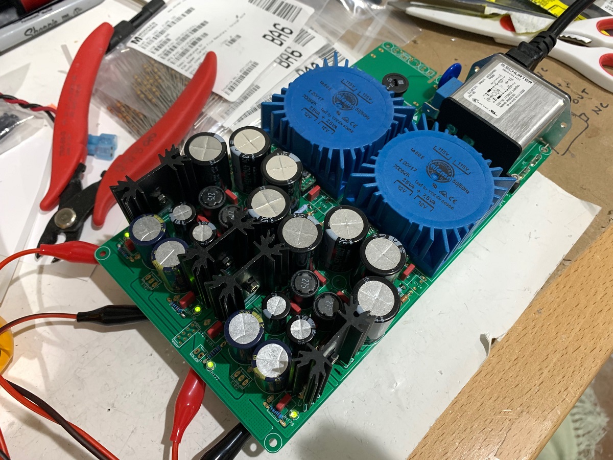
Yes, on that note... That little thing that you see on the right which is powering your amp is a BJT based cap multiplier fed from LM317/337 regulator implemented in low noise application: Simple Voltage Regulators Part 1: Noise - [English] and https://electrooptical.net/static/oldsite/www/sed/ErrolDietzRegulatorNoisePeaks.pdf. I like BJT cap multipliers as they have much less voltage drop across them. That combo looks very good on my scope, so I think I'm grand in terms of PS for now. I'll definitely populate your DC-DC converter board some day, but for now I'll stay with that supply that I have laying around. I hope that's OK . I actually have two of them, build for some other HP Amp with independent channels, but that design had quite unacceptable MOSFET bias drift so it's gathering dust now while your's is playing out loud. Bias on your amp is really nailed, it doesn't move more than +/- 2mV/2.7ohm. Good stuff!
That little thing that you see on the right which is powering your amp is a BJT based cap multiplier fed from LM317/337 regulator implemented in low noise application: Simple Voltage Regulators Part 1: Noise - [English] and https://electrooptical.net/static/oldsite/www/sed/ErrolDietzRegulatorNoisePeaks.pdf. I like BJT cap multipliers as they have much less voltage drop across them. That combo looks very good on my scope, so I think I'm grand in terms of PS for now. I'll definitely populate your DC-DC converter board some day, but for now I'll stay with that supply that I have laying around. I hope that's OK . I actually have two of them, build for some other HP Amp with independent channels, but that design had quite unacceptable MOSFET bias drift so it's gathering dust now while your's is playing out loud. Bias on your amp is really nailed, it doesn't move more than +/- 2mV/2.7ohm. Good stuff!This PSU has a cap multiplier after the voltage regulators to provide a slow ramp up soft start to prevent SMPS latching and to reduce noise even further. The cap Mx has a circa 1.5v dropout so what you are seeing is normal. You can adjust the programming resistors of the regularors to be circa 19.5v. I usually use the eBay units with a trim pot which makes it easy. The LOVDR ones tend to come in fixed values. Look at the datasheet to see the programming resistors needed on the -ve one. On the +ve one, just reset the solder jumpers for 19.5v (or whatever the dropout is). It is not critical to be exact.
Last edited:
Thanks for that link. NWAvguy seems to think that it’s HiFi phoolery. If you already have a dual rail PSU it’s not doing anything for you.
So why create a virtual ground with a 3rd channel? Remember the audiophile vibration reduction from above applied under the wrong circumstances? This is essentially the same thing—a “solution” without a problem. The third diagram to the right shows the dual power supply with its real ground, and the virtual ground created from the split power supply rails.
Yes, I've been familiar with that NWAV page since he first posted it, years ago. NWAV is quite verbose about the case against virtual ground.
That said, if you do a bit of Googling, you'll see several headphone amp projects that use 3-channel (virtual ground). Indeed most of my DIY headamp projects are 3-channel.
Not sure about how many commercial amps are 3-channel.
That said, if you do a bit of Googling, you'll see several headphone amp projects that use 3-channel (virtual ground). Indeed most of my DIY headamp projects are 3-channel.
Not sure about how many commercial amps are 3-channel.
So the idea is to make 3 channels of output and have the third one drive the ground. I am not sure what this serves - it it sort of like a big servo to keep ground at 0v? A well designed amp has inherently low 0v (GND) DC offset. I can see the active ground sort of serving to make the amp behave closer to a balanced drive amp for higher damping factor.
I don’t have anymore of the full PCB sets. However, I have some of the earlier standalone amp boards that can work with a simple jumper mod. 4 of these could be used to make a balanced stereo out. PM me if interested.
A very nice PSU for this would be the Yarra Gen 2 linear supply with CRCLC and LDO regulators. This PSU has the worlds smallest LT4320 active bridges.
A very nice PSU for this would be the Yarra Gen 2 linear supply with CRCLC and LDO regulators. This PSU has the worlds smallest LT4320 active bridges.
Last edited:
- Home
- Group Buys
- Simple High Performance DC Coupled Class A HPA with sub PPM THD