Yeah, I’m gong to source some 2A devices. I really don’t trust the ones I got and seller won’t answer any questions about them. Steer clear of these: 10PCS BF862 ORIGINAL JFET N-CHAN 20V SOT-23 | eBay
Note that the photograph from that seller shows “2AW” markings!
I got mine from here and they were genuine with 2AW markings and hey work great.
Free shipping 100pcs/lot BF862,215 BF862 JFET N CHAN 20V SOT 23 Best quality-in Integrated Circuits from Electronic Components & Supplies on Aliexpress.com | Alibaba Group
Hey all, I've been working on-and-off on an NHB kit from X's Etsy store. I've been in contact with X and he asked me to post my latest troubleshooting data. I've not been able to get consistent audio out of the amp with my right channel being crackly with static. There was a time when my power LED would fade in and out but that seems mostly gone. There was also a time when I could have sworn I saw smoke but visual inspection of all my components doesn't show any evidence of burning or bulging.
I need to replace my batteries since they're sitting at close to 14.5V - 15V across both in series. With that in mind:
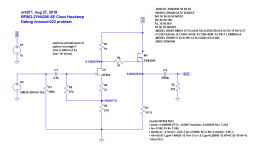
V across R3: A - 8.6V; B - 1.7V
Q Drain to GND: A - 1.96V; B - 13.56V
Q Gate to GND: A - 1.74V; B - 11.48V
Q Source to GND: A - 8.6V; B - 1.74V
M Drain to GND: A - 14.7V; B - 14.2V
M Gate to GND: A - 8.6V; B - 13.1V
M Source to GND: A - 5.86V; B - 10.2V
C1 and C2 arrays are doing their job in that no DC is measured on R1 or RL.
Thanks to everyone for the input and expertise.
I need to replace my batteries since they're sitting at close to 14.5V - 15V across both in series. With that in mind:
V across R3: A - 8.6V; B - 1.7V
Q Drain to GND: A - 1.96V; B - 13.56V
Q Gate to GND: A - 1.74V; B - 11.48V
Q Source to GND: A - 8.6V; B - 1.74V
M Drain to GND: A - 14.7V; B - 14.2V
M Gate to GND: A - 8.6V; B - 13.1V
M Source to GND: A - 5.86V; B - 10.2V
C1 and C2 arrays are doing their job in that no DC is measured on R1 or RL.
Thanks to everyone for the input and expertise.
Code:
V across R3: A - 8.6V; B - 1.7V
Q Drain to GND: A - 1.96V; B - 13.56V
Q Gate to GND: A - 1.74V; B - 11.48V
Q Source to GND: A - 8.6V; B - 1.74V
M Drain to GND: A - 14.7V; B - 14.2V
M Gate to GND: A - 8.6V; B - 13.1V
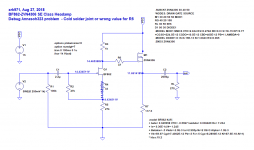
M Source to GND: A - 5.86V; B - 10.2VI ran two sims with 15v Vcc, one case for channel A (good) and the DC setpoints appear to be consistent with what you have.
Second case, I made R5 100x bigger (perhaps you have an incorrect value there or it has a cold solder joint?). That produces DC setpoints consistent with what you measure. This condition has very weak bias in JFET and too much bias in MOSFET and will sound crackly and distorted.
My suggestion is to remove R5 and replace with a new 270R. Retouch solder points after JFET (R4, R5, JFET pin S).
That should fix channel B.
Attachments
Thanks for running the sims (the sim software I used to use in my college days was provided through the school; what's popular around here that's free/not expensive?). I do recall desoldering certain components and it seemed like the solder pad on the component had maybe gotten damaged. It's possible I did it again with R5. I'll poke around and report back.Code:V across R3: A - 8.6V; B - 1.7V Q Drain to GND: A - 1.96V; B - 13.56V Q Gate to GND: A - 1.74V; B - 11.48V Q Source to GND: A - 8.6V; B - 1.74V M Drain to GND: A - 14.7V; B - 14.2V M Gate to GND: A - 8.6V; B - 13.1V M Source to GND: A - 5.86V; B - 10.2V
I ran two sims with 15v Vcc, one case for channel A (good) and the DC setpoints appear to be consistent with what you have.
Second case, I made R5 100x bigger (perhaps you have an incorrect value there or it has a cold solder joint?). That produces DC setpoints consistent with what you measure. This condition has very weak bias in JFET and too much bias in MOSFET and will sound crackly and distorted.
My suggestion is to remove R5 and replace with a new 270R. Retouch solder points after JFET (R4, R5, JFET pin S).
That should fix channel B.
Thanks for running the sims (the sim software I used to use in my college days was provided through the school; what's popular around here that's free/not expensive?). I do recall desoldering certain components and it seemed like the solder pad on the component had maybe gotten damaged. It's possible I did it again with R5. I'll poke around and report back.
I haven't had a shot at my soldering iron yet but I did probe my R5 with my DMM. Strangely, both A and B are showing the same resistance in the neighborhood of 240Ohms. It could be related to the odd charging/discharging type behavior I measure between gnd and vcc. I also measured from points electrically equivalent to but not on the resistor itself to check for a cold joint. A bit odd. I will still try to go at it with my iron but the measurements as of now don't seem to indicate a bad joint/R5.
Alright, combination of good, bad, and neutral news. Good news is that after fiddling with R5 and other miscellaneous poking with the iron, it seems like the problem may be solved! My resistance measurements were good so I hooked up the batteries and to check DC and the DC values on both channels looked to be in sat range. I plugged in headphones to the output and no crackling, just silence.
Bad news is that I don't have an aux cable with me to actually play music which is what I'd really love to do. First thing when I get home will be to grab my aux dongle, swipe a fresh pair of batteries, and start test driving. After that (if there is an after) will be to try punching the holes into the Altoids tin for a proper installation. Hopefully. Hinges on confirmation of success. So, so, so close now.
Miscellaneous notes:
- Never did really figure out what the problem was. None of my solder joints looked good but none of them really seemed bad. To verify R5, I managed to desolder it and ever so carefully probed it to make sure it was sat to spec. Seemed like it was so I carefully placed it back and soldered it on. Before and after, the resistance I probed from point to point on the PCB never changed.
- I did touch up a couple of other points on the JFET. Before and after, resistance from D to S was around 30 or 31 Ohms. Again, not sure if what I did here was to blame. When doing yesterday's and today's measurements I would try, as much as possible, to probe the solder points directly and also an electrically equivalent point as well to verify. Never really did figure out a difference.
Summary of my experience (just the parts that worked) for those that might just have searched the word "troubleshoot" looking for help:
- Soldered up, crackling noise from one channel.
- Measured DC voltages at various nodes, particularly JFET and MOSFET pins to gnd.
- Compared to X's sims that show DC bias points.
Per X's diagnosis, focus was on R5 and JFET nodes. Measured resistances: R5 resistance ~270Ohms, JFET drain to JFET source /= 0 (or short).
- Re-touched soldered points. Profit?
JFET drain to source should be about 30ohms not a short 0ohms. If it is, you either have a solder bridge or a bad JFET. Don’t worry you will solve it - it is a simple circuit and not much can go bad. Another place to check is make sure those 0.1uF X7R caps are not shorted. Measure across them with ohm meter and should not be 0ohms.
JFET drain to source should be about 30ohms not a short 0ohms. If it is, you either have a solder bridge or a bad JFET. Don’t worry you will solve it - it is a simple circuit and not much can go bad. Another place to check is make sure those 0.1uF X7R caps are not shorted. Measure across them with ohm meter and should not be 0ohms.
Sorry, I did mean to indicate that. I do have about 30 Ohms between JFET D and S. I tried to indicates "not equals" with a "/=". I thought it should be around 30 Ohms but couldn't remember if that figure was truly accurate so I didn't want to mislead people by quoting 30 Ohms when I wasn't sure. But, you've confirmed it.
Plugging things now and... shoot. Still crackling. Okay, back to my meter to double check my voltage figures. It seems my earlier measurements were slightly deceptive. For some reason, the voltages on channel B are swinging. As an example, MOSFET G pin was around 8.5 V (using my same 15V batteries) and dipping down, sometimes as low as 3.5V. I'll recheck my solder points for a possible intermittent connection. Is there any other way to verify JFET?
If current through R3 is correct, JFET is good. If not, and all solder joints are good, it’s a bad JFET.
Is a possible symptom of a bad JFET a variable DC voltage? Starting at 8V then dipping down? I can't think of any other component that would do that.
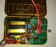
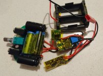
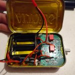
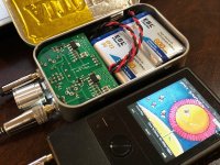
Final (for now I think?) build.
3300 uf on rails as well as outputs, outputs with KA & 1u wima bypass.
2x18350s for power @ 1200mAh per cell. Running at a hair under 70mA
Only thing is the jst for the battery holder is a bit thick when stuffed in and lid closed, but I wanted the battery holder easily taken out for replacing batteries etc
Attachments
Final (for now I think?) build.
3300 uf on rails as well as outputs, outputs with KA & 1u wima bypass.
Nice! Capacitor P*rn!

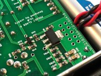
New MOSFET: ZXMN10A08GTA
The originally spec'd ZVN4306GTA's, although a fine performer for several years now, may becoming EOL as out of stock at Mouser for some time now. In looking for a suitable alternative, a ran across the ZVMN10A08GTA from same manufacturer (Diodes Inc) and it has a much higher transconductance figure gfs, higher voltage rating, and higher current rating and still same SOT-223 package. I decided to give it a try and they indeed sound great. Although I have not measured it yet, the higher transconductance should make it work better with lower impedance headohones and provide even a higher damping factor (more authority to drive difficult headphones).
https://www.diodes.com/assets/Datasheets/ZXMN10A08G.pdf
If you have a hot air gun, it is relatively easy to desolder the ZVN4306GTA and replace with new ZXMN unit. I matched mine of course.
On my shop, I will be switching to this new MOSFET as standard now and they will also be the MOSFETs provided in the matched FETs package.
The markings are so faint, you have to look at it in the right light to see it. Here you can see them swapped out of the old amp - the heat gun makes for clean swap/replacement work.
Attachments
Thanks StellarE, the hot air gun is only $40 on Amazon and totally useful for anyone doing SMT soldering/rework. Solder paste in a syringe with hypo needed is also key, as well as fine copper braid for removing old solder to provide a flat pad for new soldering.
If you do a lot of work on SMT, having the iExtruder is also very handy, I have it and love it but if you have just a few parts like this amp then it is not justified.
If you do a lot of work on SMT, having the iExtruder is also very handy, I have it and love it but if you have just a few parts like this amp then it is not justified.
Neat update. I can't believe it's been nearly half a year since the last time this thread has had traffic.In looking for a suitable alternative, a ran across the ZVMN10A08GTA from same manufacturer (Diodes Inc) and it has a much higher transconductance figure gfs, higher voltage rating, and higher current rating and still same SOT-223 package.
Are these purely one-for-one swaps? I had to remind myself that the first stage was the voltage gain stage and so changing out the MOSFET wouldn't have an appreciable difference there. I'm assuming the resistor biasing network stays largely the same since the voltages should be the same as well. I know some would tweak the network to get a bit more output current. Since the transconductance is higher, are we basically getting more current without changing the voltages? All else being equal, will battery life also take a slight dip?
The current is a function of the individual MOSFET gain and very similar to the ZVN4306. I measured about 24 of them in-situ and there were variations but for the most part, had a bit less current flow for same resistor network. I ended up at 54mA which is fine. My amp was running kind of high at 70mA before but that because of a “hot” ZVN4306. You battery usage will track with current and 54mA is good for about 4.5hrs to 5hrs.
- Home
- Group Buys
- xrk971 Pocket Class A Headamp GB