That thought did cross my mind and I double checked the markings just to make sure they were the GR bin. I also went though and measured the 10x 209GRs I got from Mouser (for matching) and most were within 0.5V of each other, generally giving 3.5-4V across R3.
So what you're saying is you'd suggest leaving R4/R5 at/closer to specified values and try to vary R3 instead?
In that case probably I'd need a larger R3?
Since I'd need to bring voltage at mosfet gate down - with values as specified on the diagram R3-R6 junction measures at 13.9V..
Also, my previous post should have read: "Voltage at R4-R5 junction was 1.20/1.21V and R3-R6 was 12.37/12.38V"
Last edited:
If the simulation shows THD to be less than 0.06% with dominant H2 vs H3 then either can work if it achieves that. I think something like 47R for R4 and adjust R3 to get the circa 60mA to 70mA bias and a DC midpoint near 8.5v to 9v is best. Feel free to play with the source resistor value to achieve the above goals.
Hi X,
I TRIED to follow (noob) your schematic for PCA and the latest BOM but I don't know how much have I messed it up (I probably did something wrong).
Would you be kind to check it and correct it (or point me in right direction - I am more than willing to learn) when/if you have time.
Thanks in advance,
Mladen
Attachments
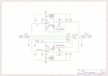
Looks good to me. Your 2Sk209gr is an N-ch JFET. You have an N ch MOSFET symbol there by mistake. Not that it would matter. Regarding resistor values, if this is what you got from the latest BOM for use with 2SK209GR then it’s good. There are different values for 2SK209BL. You don’t need 270ohm RLA/B. That’s the dummy load of the headphone. The 1k is a sufficient output cap drain cap.
Yeah, I followed resistor values for 2SK209GR. Regarding the symbol I think that's EasyEDA fault (but I'll check it). So the only mistake I made is that RLA/B - Yay me ")
Thank you so much for a quick reply!
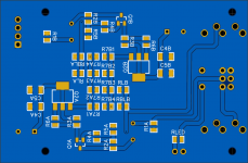
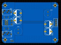
This is the layout I've done so far:
Thank you so much for a quick reply!
This is the layout I've done so far:
Attachments
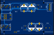
Note that the MOSFETs need extra copper surface area from pin 4 to dissipate the heat it generates. It makes about 500mW so needs a way to remove the heat. On my board, there is some extra copper to radiate heat away from pin 4 (the tab).
The four 470ohm resistors also make a lot of heat so need some space and room to breathe.
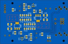
You can see the copper pad extended out from pin 4 of the MOSFETs that act as heatsinks:
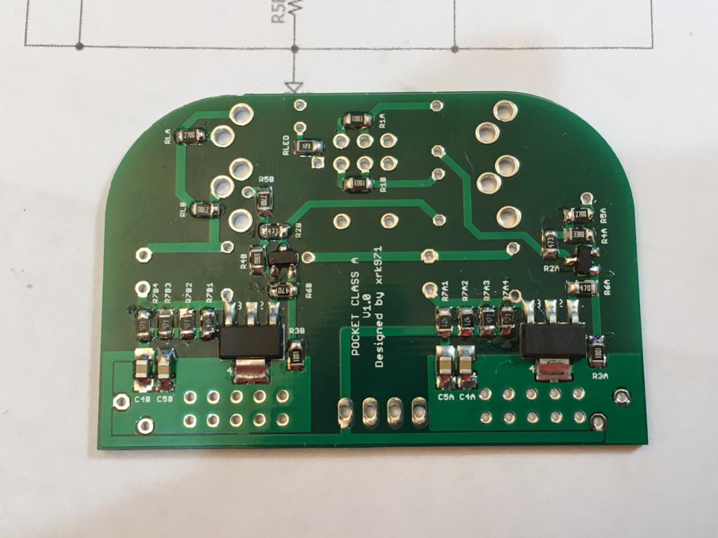
Those copper pads connected to the tab of the MOSFET are at battery positive potential. Needs to be isolated from ground. Look at the rectangles with vias in them to thermally bond both sides of the PCB to increase thermal dissipation. Those rectangles with the holes are at +Vcc and act as heatsink.
Like this:

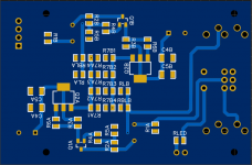
Your layout is concentrating the heat in the middle of the board with the 8 source resistors clustered need the middle. They will get hot. Better to spread them out, on opposite sides of board if possible.
Like this:
Your layout is concentrating the heat in the middle of the board with the 8 source resistors clustered need the middle. They will get hot. Better to spread them out, on opposite sides of board if possible.
Attachments
Last edited:
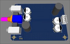
So, I rearranged components as you've suggested. MOSFETs and 470 resistors are on opposite sides of the board and I added copper pads (on both sides) for heat dissipation.
Is there anything else I've missed, or could've done differently?
Sincerely,
M
Is there anything else I've missed, or could've done differently?
Sincerely,
M
Attachments
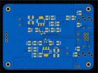
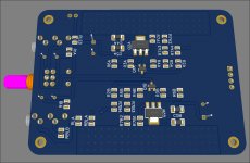
The thermal pad look good for the mosfet. The spacing looks good for the heat. Probably doesn’t need to extend under central portion which could be via double plane ground to cool the 470R x4 resistors. Can you show schematic again? I don’t know why it appears R7A1/2 or R7B1/2 connects to positive rail on thermal radiator? Also, what is R2/4/5 doing?
Hello,
Do you guys share eagle or gerber files? I like the less compressed version and would order PCB to try it.
I would have a question on PSU. The last solid state headphone amp I made is a CK2III and when I did run it from an old HP6624A and no matter what PSU I made, even SLA battery, it was not as good as the old monster rack PSU. For a while I have used it with the monster PSU, but it was a pain to type the voltage an current values each time I switch on, not speaking about the size of it.
This one I would run from battery, but what battery? Did you guys experimented with LiPO packs? Maybe a 6S LiPo pack would do the job better, with lower internal resistance etc. I have no idea if that sounds better, but unless you guys say it is not good, I would try.
Thanks a lot!
JG
In this thread, I show how to use a 3000mAhr LiPo with DCDC step up and cap Mx for a soft start. It works very well and sounds same as 9v Li-ion Battery.
MladenGavric,
If you want to continue on this amp or to share your own Gerbers, please start a new thread as this is specific to my design and GB/store. The schematic and topology is open source and anyone can make it if they please.
Giordano,
If you like this topology but want a more open layout, try the DCA (desktop Class A) amp. It’s the same amp but bigger and suited for cap rolling and has built in cap Mx PSU.
It lets you use one big fat LiPo cell and easy to charge with a 5v USB auto-charger module ($1). A small DCDC is $1 and provides constant adjustable voltage invariant of battery voltage.
To get 18v would require about 5s battery. The only chargers for a 5s that is a special RC race car/quad copter charger (pricey and bulky).
To get 18v would require about 5s battery. The only chargers for a 5s that is a special RC race car/quad copter charger (pricey and bulky).
Last edited:
Well the switch on my pot failed and getting it out pulled out most of the vias so I've got a little project on my hands. Couldn't get the solder out with the sucker or wick and ended up melting bismuth into a giant blob and sliding the pot out while the blob was liquid.
I figure while I'm at it I'd redo the whole the board as I've amassed a collection of better components since the build (pretty sure I even used thick film resistors and some cheap jacks) including matched FETs.
I've been reading the thread to refresh my memory and some stuff is still a little nebulous to me.
I have 10uF Silmic II on the input. I don't see them in the BOM. What was the reasoning for this again? I do remember testing them with Wima bypass and not liking the result.
I'll be using low impedance phones (~16Ω) mostly.
Thanks, I'm sure I'll have more.
- Home
- Group Buys
- xrk971 Pocket Class A Headamp GB