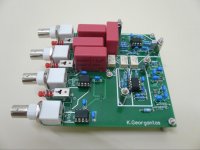
I've been working on this for about a year and still incomplete but almost done. I couldn't hold myself to post some first pics.
Actually, it has been quite some time I'm fooling around low cost soundcards trying to modify them for improved performance. What strikes me is that although manufacturers don't hesitate to use top class chips, the overall performance is compromised by design. For example the power supply even if it's not the USB Vbus, it will be just a small external wall wart. Another problem is the necessity for a user friendly front panel which leads to a messy PCB layout. And then it comes the copyright war forcing companies to adopt proprietary solutions especially in the software domain, causing even instability issues in some cases. Most of the time I came to think what if app notes were followed to the letter but this would take a complete redesign from scratch. Eventually it happened.")
I rush to catch up any queries. This is not meant to be a giant killer. In fact, I deliberately stayed within limited bandwidth and dynamic range to avoid meeting spooky shadows. The target was the low to mid cost commercial soundcards. That said, it costs more than a Focusrite Scarlet to build and one might think that it doesn't manage any better. But all these products need some kind of input protection and usually adding that will also add THD+N. So, my soundcard is ready to accept an amplifiers output, the loop measurement are taken on these inputs and the total cost is much less than a soundcard-input interface combo. And it's mine, which is priceless...
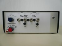
About specifications: Two channels -stereo- full balanced I/O. Input impedance 100k. Input sensitivity for 0dBFS 1,5Vrms differential. Input protection for 400VDC. Also it should be OK for 100Vp AC but I haven't tested that. Output can drive most usual loads with a max 2,6Vrms differential. Full duplex up to 192kHz/24bit, but usable only at 48kHz with ARTA, REW and the alike.
Still on the bench, I expect a little more improvement when I put it in the box. I verified that at least for the 50Hz noise. Lock down delays but it shouldn't take long more. I'll share all schematics and gerber files for anyone who needs something like that and can build it.
Actually, it has been quite some time I'm fooling around low cost soundcards trying to modify them for improved performance. What strikes me is that although manufacturers don't hesitate to use top class chips, the overall performance is compromised by design. For example the power supply even if it's not the USB Vbus, it will be just a small external wall wart. Another problem is the necessity for a user friendly front panel which leads to a messy PCB layout. And then it comes the copyright war forcing companies to adopt proprietary solutions especially in the software domain, causing even instability issues in some cases. Most of the time I came to think what if app notes were followed to the letter but this would take a complete redesign from scratch. Eventually it happened.
I rush to catch up any queries. This is not meant to be a giant killer. In fact, I deliberately stayed within limited bandwidth and dynamic range to avoid meeting spooky shadows. The target was the low to mid cost commercial soundcards. That said, it costs more than a Focusrite Scarlet to build
and one might think that it doesn't manage any better. But all these products need some kind of input protection and usually adding that will also add THD+N. So, my soundcard is ready to accept an amplifiers output, the loop measurement are taken on these inputs and the total cost is much less than a soundcard-input interface combo. And it's mine, which is priceless...About specifications: Two channels -stereo- full balanced I/O. Input impedance 100k. Input sensitivity for 0dBFS 1,5Vrms differential. Input protection for 400VDC. Also it should be OK for 100Vp AC but I haven't tested that. Output can drive most usual loads with a max 2,6Vrms differential. Full duplex up to 192kHz/24bit, but usable only at 48kHz with ARTA, REW and the alike.
Still on the bench, I expect a little more improvement when I put it in the box. I verified that at least for the 50Hz noise. Lock down delays but it shouldn't take long more. I'll share all schematics and gerber files for anyone who needs something like that and can build it.
Attachments
Thanks! A few more general info. The design is based strictly on app. notes and realized with free software. So, there were some restrictions regarding the PCB complexity. That's why I split it to three decks keeping dimensions at 100x100mm to take advantage of the PCB manufacturers' offers. Consequently, the connectors/switches layout is a bit shrunk but I have no problem to use them. I tried to minimize SMD parts only to a few chips. The rest is THT parts. Finally, it needs a USB to I2S input and output converter which is not my design.
I assume you're asking about the USB interface and that's a good question. I'm using a DIYINHK module that I purchased in the early summer. I can't find the exact model in their catalogue but its pretty similar to this only mine has a "B" type USB port. XMOS Multichannel high-quality USB to/from I2S/DSD SPDIF PCB - DIYINHK When I was searching for this I couldn't find much alternatives, but I remember there was another module from MiniDSP which I can't find now.
So, it might be useful to start from the USB interface. Not much to say about that... Being completely unable to write code I tried to copy a commercial design with no luck. Behringer UMC 202HD for measurements Then I had to find out how to use the DIYINHK module. You can read here for some laughs! CS4272 stuck in power down mode The good thing -if at all- is that only I2S is needed, not I2C. That means there are no auto functions, even sampling rate is set manually with a rotary switch. It works fine for me and it makes things a lot easier to cooperate with any USB interface. Commercial or DIY... but I can't help with that.
EDIT: I found the MiniDSP module MCHStreamer - USB Audio Swiss-Army knife - Multichannel PCM/DSD/PDM/ADAT/TDM/SPDIF interface
CS4272 stuck in power down mode The good thing -if at all- is that only I2S is needed, not I2C. That means there are no auto functions, even sampling rate is set manually with a rotary switch. It works fine for me and it makes things a lot easier to cooperate with any USB interface. Commercial or DIY... but I can't help with that.EDIT: I found the MiniDSP module MCHStreamer - USB Audio Swiss-Army knife - Multichannel PCM/DSD/PDM/ADAT/TDM/SPDIF interface
Last edited:
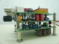
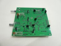
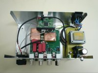
Construction part I: the PSU (lower deck)
As the circuit was growing up, it was clear that the USB Vbus wouldn't suffice. Of course there are DC boosters but the current consumption could not be supported even if two USB ports were occupied. So, I went for a proper linear psu. A 2x12 toroid with magnetic shield to bridge rectifier and capacitor bank. I managed to squeeze some bigger than the original thought at the bottom of the PCB. Then it splits to regulators for 3,3V, 5V +/-8V and +/-12V. Full LT3042/94 job. I can't tell if this is an unnecessary overkill. Maybe plain LM78xx could do it. I just wanted to keep this factor out of the equation. Big words. Those little bugs are said to be very itchy... That's why I didn't use those modules found here and there despite that it would be easier and cheaper. I tried to follow the datasheet recommendations and crossed fingers. If anything else, this thing can measure itself for noise...
The PCB layout seems a bit awkward. That's because I placed each regulator right under the chip it feeds on the next deck to eliminate power rails. It is connected with pin headers. An easy way to align them is to use the long pins type, put them in place -male to the lower deck, female to the next- and press gently the boards to sit on the 12mm metal spacers. Then solder everything and cut the remainings of the pins at the bottom.
I attach the schematic. I used 50ppm metal film resistors and X7R MLCC caps. Two of the regulators are not on this PCB but on the top one. Also attached gerber files.
Attachments
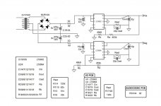
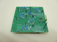
Construction part II: AudioCodec and buffers (mid deck)
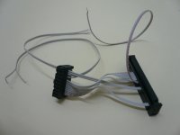
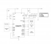
CS4272 configured in stand alone mode. Sampling rate set with a 2pole/4pos rotary switch. Everything is on the schematic. Connects to the USB module with a 2x8 pin header. This is not very straightforward. Use the PCB markings to find your way. I attach a photo of this. Each line needs a gnd pair and the total length should not exceed 10cm. Except the loose wires which are taking M0/M1 to the rotary switch together with 3,3V and gnd and RST to a button , the only things wired off board on the front panel.
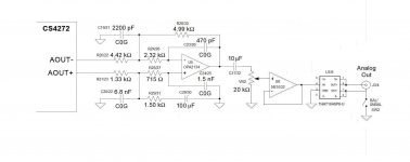
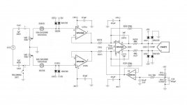
The output stage is taken from CS4272 datasheet. I only increased the electrolytic caps C29/30 to extend the low frequency roll off. Then it goes to a 20k pot salvaged from my UMC202. Poor donor... But I'll always remember it as the final and most important step before I jump on this project! For special parts I'll make a small BoM in another post. After the pot there is a necessary buffer and then the balanced drivers. I used THAT1646 but DRV134 will do fine. These drivers are not on this deck but on the top one.
The input stage was the real challenge! Actually, you are looking at the PCB v.3. I tried a few schemes. The opa1632 was there from the beginning. There is an app note on the datasheet right on spot. I just copied that. The problem with ADC buffers are their input or antialiasing caps, a heavy load for opamps. Here's a good read: Op Amps Driving Capacitive Loads | Analog Devices Theoretically, every opamp could be compensated but there will be an impact on performance. OPA1632 does fine in this position. But alone is not able to hold a high impedance attenuator plus overvoltage protection. I tried a few buffers (opamps and INA) with the pots in SE and balanced -U shape if you prefer- configuration. Attached is the scheme that works best. The attenuator is a 4gang pot. I don't like the stepped switches as they won't allow for fine adjustment to 0dBFS.
About the input protection scheme. I hope I did something meaningful here. The incandescent lamps draw 5mA already at 9V. Anyway, they should hold some defense. The input caps are on the top deck. There also diode clamps at the ADC input because the opa1632 can swing a lot more that absolute max. However, there are no current limiters here. I thought the positive rail can do hardly 1V on the diodes and the negative rail sinks to gnd. Please check sanity.
Vcom comes from a voltage divider to a DC buffer. Do not use the Vcom from the CS4272 for this job. It doesn't like it at all! Bypass this with 1μF and leave it alone.
Gerber files attached.
CS4272 configured in stand alone mode. Sampling rate set with a 2pole/4pos rotary switch. Everything is on the schematic. Connects to the USB module with a 2x8 pin header. This is not very straightforward. Use the PCB markings to find your way. I attach a photo of this. Each line needs a gnd pair and the total length should not exceed 10cm. Except the loose wires which are taking M0/M1 to the rotary switch together with 3,3V and gnd and RST to a button , the only things wired off board on the front panel.
The output stage is taken from CS4272 datasheet. I only increased the electrolytic caps C29/30 to extend the low frequency roll off. Then it goes to a 20k pot salvaged from my UMC202. Poor donor... But I'll always remember it as the final and most important step before I jump on this project! For special parts I'll make a small BoM in another post. After the pot there is a necessary buffer and then the balanced drivers. I used THAT1646 but DRV134 will do fine. These drivers are not on this deck but on the top one.
The input stage was the real challenge! Actually, you are looking at the PCB v.3. I tried a few schemes. The opa1632 was there from the beginning. There is an app note on the datasheet right on spot. I just copied that. The problem with ADC buffers are their input or antialiasing caps, a heavy load for opamps. Here's a good read: Op Amps Driving Capacitive Loads | Analog Devices Theoretically, every opamp could be compensated but there will be an impact on performance. OPA1632 does fine in this position. But alone is not able to hold a high impedance attenuator plus overvoltage protection. I tried a few buffers (opamps and INA) with the pots in SE and balanced -U shape if you prefer- configuration. Attached is the scheme that works best. The attenuator is a 4gang pot. I don't like the stepped switches as they won't allow for fine adjustment to 0dBFS.
About the input protection scheme. I hope I did something meaningful here. The incandescent lamps draw 5mA already at 9V. Anyway, they should hold some defense. The input caps are on the top deck. There also diode clamps at the ADC input because the opa1632 can swing a lot more that absolute max. However, there are no current limiters here. I thought the positive rail can do hardly 1V on the diodes and the negative rail sinks to gnd. Please check sanity.
Vcom comes from a voltage divider to a DC buffer. Do not use the Vcom from the CS4272 for this job. It doesn't like it at all! Bypass this with 1μF and leave it alone.
Gerber files attached.
Attachments
That said, it costs more than a Focusrite Scarlet to build
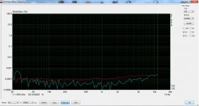
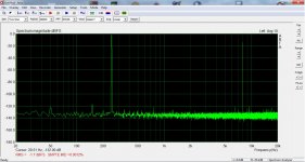
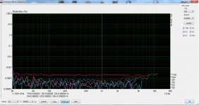
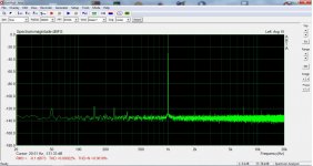
Oh it is quite a bit better! Maybe not on noise floor, but definitely on distortion!
0.00022 at -0.1db output is very impressive to me! edit: and I suspect it is actually better than that. the 7K and 9K spikes I see from time to time, some sort of outside interference I think. If you did the test at say 990Hz I'm guessing your distortion figure will be lower, as at present it is probably registering that 7k and 9k as 7th and 9th harmonics, and I don't believe that is what they are.
Tony.
Last edited:
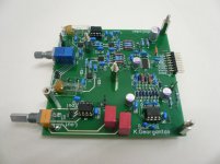
Construction part III: I/O and high gain preamp (top deck)
I used BNC because they are universal and space saving. Two inputs two outputs with a switch between each pair to select bal/unbal in or out. Another switch right in the middle between inputs/outputs to select mono/dual channel i.e. connects the left out to the right in. Also, here are the input caps -the biggest PP I could squeeze- and the output drivers, as explained in the previous post.
And then there was plenty of room left. So, I added a high gain preamp. No fancy designs, no unobtainiums. Rod Elliott's P158 Project 158 with LME49720 -because I had them. Consequently, the output cap of the first stage should be reversed. The gain selection is done with microrelays salvaged from another victim of my experiments. And a 3pole/4pos rotary switch to control them wired on the front panel. The preamp has a dedicated psu and a shield made from copper foil, the type for artist's work.
I haven't played with this so far. I need to put it in a box and then do the 1k resistor test suggested by Rod.
I can't remember of anything else at the moment. I think I'll have it ready by the weekend.
I used BNC because they are universal and space saving. Two inputs two outputs with a switch between each pair to select bal/unbal in or out. Another switch right in the middle between inputs/outputs to select mono/dual channel i.e. connects the left out to the right in. Also, here are the input caps -the biggest PP I could squeeze- and the output drivers, as explained in the previous post.
And then there was plenty of room left. So, I added a high gain preamp. No fancy designs, no unobtainiums. Rod Elliott's P158 Project 158 with LME49720 -because I had them. Consequently, the output cap of the first stage should be reversed. The gain selection is done with microrelays salvaged from another victim of my experiments.
And a 3pole/4pos rotary switch to control them wired on the front panel. The preamp has a dedicated psu and a shield made from copper foil, the type for artist's work. I haven't played with this so far. I need to put it in a box and then do the 1k resistor test suggested by Rod.
I can't remember of anything else at the moment. I think I'll have it ready by the weekend.
Attachments
Last edited:
Oh it is quite a bit better! Maybe not on noise floor, but definitely on distortion!
0.00022 at -0.1db output is very impressive to me! edit: and I suspect it is actually better than that. the 7K and 9K spikes I see from time to time, some sort of outside interference I think. If you did the test at say 990Hz I'm guessing your distortion figure will be lower, as at present it is probably registering that 7k and 9k as 7th and 9th harmonics, and I don't believe that is what they are.
Tony.
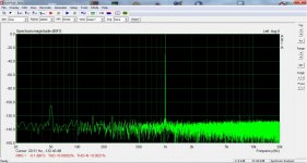
I have to address some things in the final implementation like the placement of the transformer. Also, I'm in the process of building a linear psu for the usb interface. Currently I use a SMPS and I have the feeling that it is the culprit for those spikes.
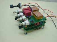
It's big...
I put some more work on this. The usb interface is quite demanding. 3,3V/800mA calls for a SMPS but forget about the cheap wall warts. OTOH, ultra low noise psu is not really needed here. I built a plain linear one with a 6V/2A transformer and LD33V with decent heatsink.. It doesn't even need a pcb, although I etched one at home. Front panel lettering is printed on metalized adhesive labels.
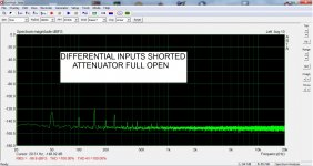
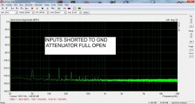
Still not finished... It's picking noise and it's not the transformers proximity to blame for that. I think it is the light bulbs at the input. I'm searching for a better solution. They pick the 50Hz plus 100Hz of lower magnitude and then spread it all over the place! The high frequency spikes are following the fundamental. 6th harmonic is supposed to set THD yet does not appear on the FFT. Maybe this is the limit of the humble CS4272 but honestly I can leave fine with that.
EDIT: It is D6+. I need new eye glasses
I put some more work on this. The usb interface is quite demanding. 3,3V/800mA calls for a SMPS but forget about the cheap wall warts. OTOH, ultra low noise psu is not really needed here. I built a plain linear one with a 6V/2A transformer and LD33V with decent heatsink.. It doesn't even need a pcb, although I etched one at home. Front panel lettering is printed on metalized adhesive labels.
Still not finished... It's picking noise and it's not the transformers proximity to blame for that. I think it is the light bulbs at the input. I'm searching for a better solution. They pick the 50Hz plus 100Hz of lower magnitude and then spread it all over the place! The high frequency spikes are following the fundamental. 6th harmonic is supposed to set THD yet does not appear on the FFT. Maybe this is the limit of the humble CS4272 but honestly I can leave fine with that.
EDIT: It is D6+. I need new eye glasses
Attachments
Last edited:
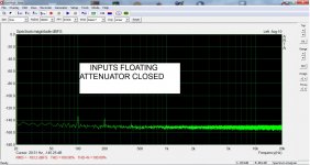
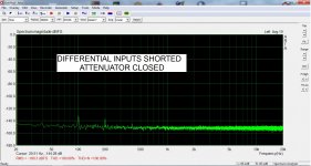
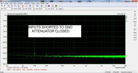
In the first 3 photos, I see only 100 Hz and its harmonics. No 50 Hz is present.
To my opinion this is due to noise from the power supply lines or noise from the grounding of the circuit.
In the other 2 photos, I see 50 Hz and 100 Hz.
But the 50 Hz and its harmonics are much bigger.
To my opinion this means that the circuit picks-up noise from the mains. Try to find why by using a lower value potentiometer (10 k ?) or to remove the bulbs or to shield better.
- Home
- Design & Build
- Equipment & Tools
- DIY soundcard intended for measuring amplifiers