This tester was developed as a spinoff from this thread:
https://www.diyaudio.com/forums/sol...collector-current-hfe-tester-transistors.html
The circuit proposed proved too complex for the OP, but I decided to bring it to completion anyway: it is probably a useful piece of kit for many DIYers.
The complexity, especially in its finished form, might look daunting, but that's kind of inevitable with this type of instrument: many parameters need to be made variable, and being a transistor tester, it has to accommodate both sexes, which brings another layer of complexity.
That said, the complexity is relative, and no expensive component is required.
It can be built as a naked board, with an external supply and multimeters as indicators, or as a complete, self-contained instrument (or anything in-between).
It does have some attractive features: it covers most of the needs for DIY use, with an Ic range of ~150µA to 1.5A, a Vce of 0 to 10V, requires a single unipolar supply, and the switches for the range and polarity are ordinary DPDT types (one has a center OFF).
A constant Ic tester is very convenient compared to alternatives improvised with supplies for example: comparisons are immediate and straightforward.
The direct-reading is also very convenient.
I didn't build and test a complete instrument: I just breadboarded the functional core for NPN (which operated as expected), and I also tested critical sections, like the polarity handling meaning the project is relatively safe.
The complete instrument has been tested in sim, and is functional (I include the .asc).
Note that this is a DIY-grade instrument, not a lab reference, but with care in construction and a good calibration, it is OK for a +/-1% accuracy, which is ample for a parameter like β.
Comparisons can be made with a greater accuracy.
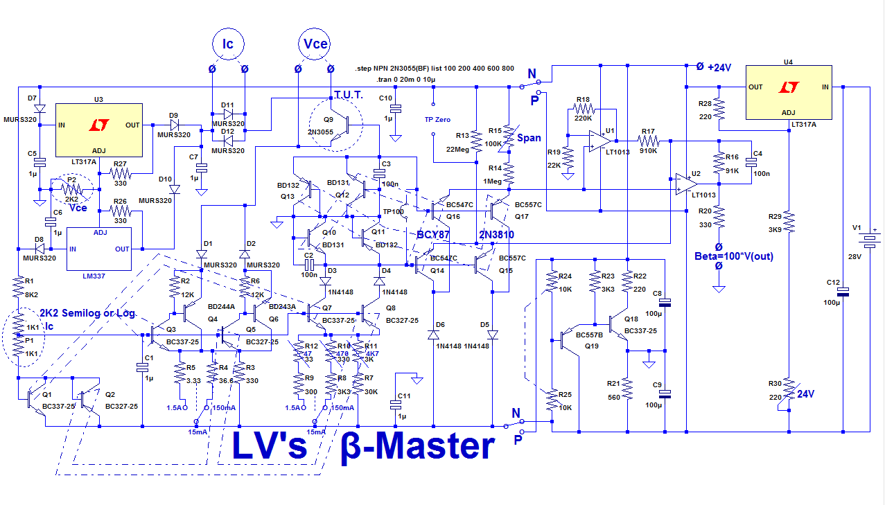
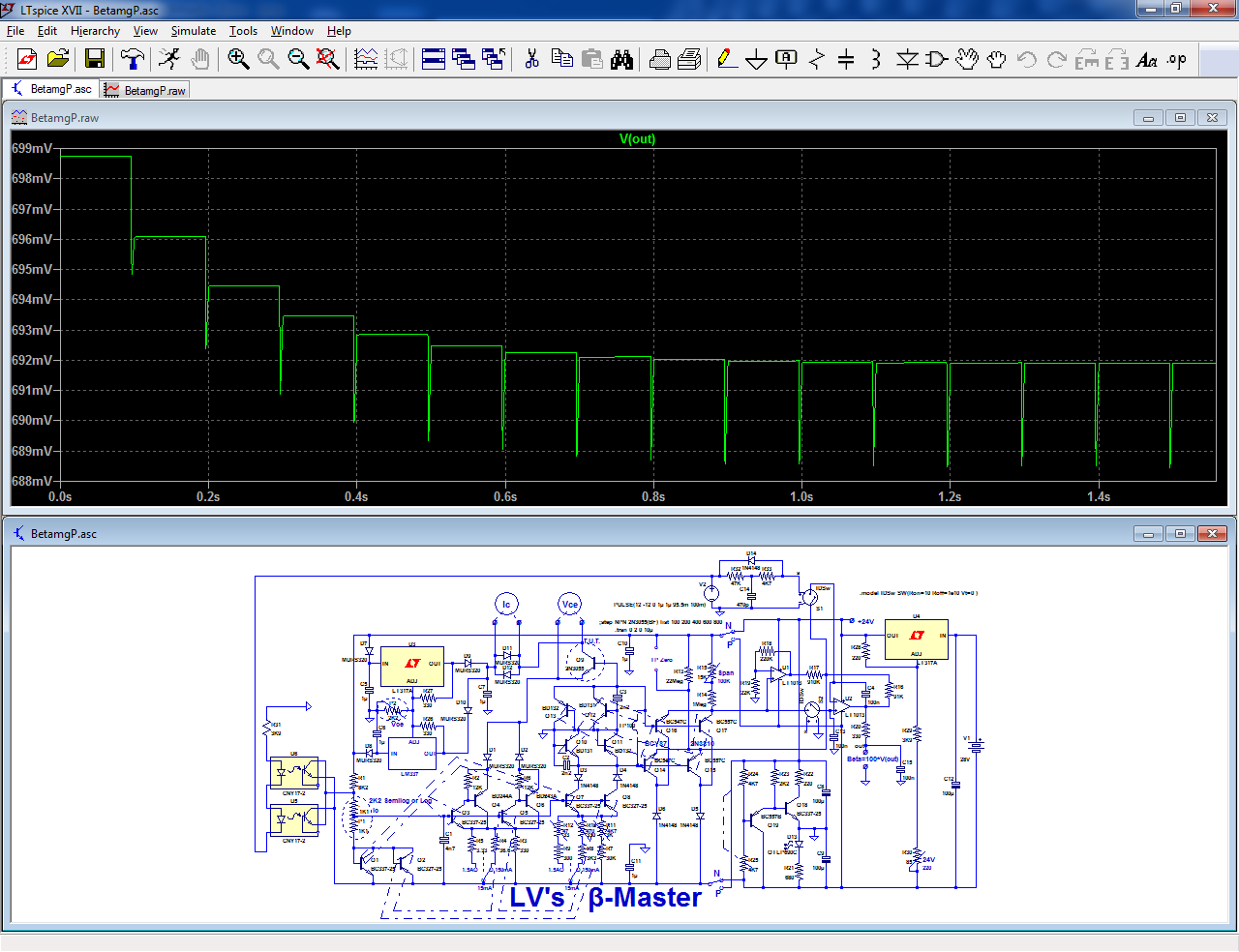
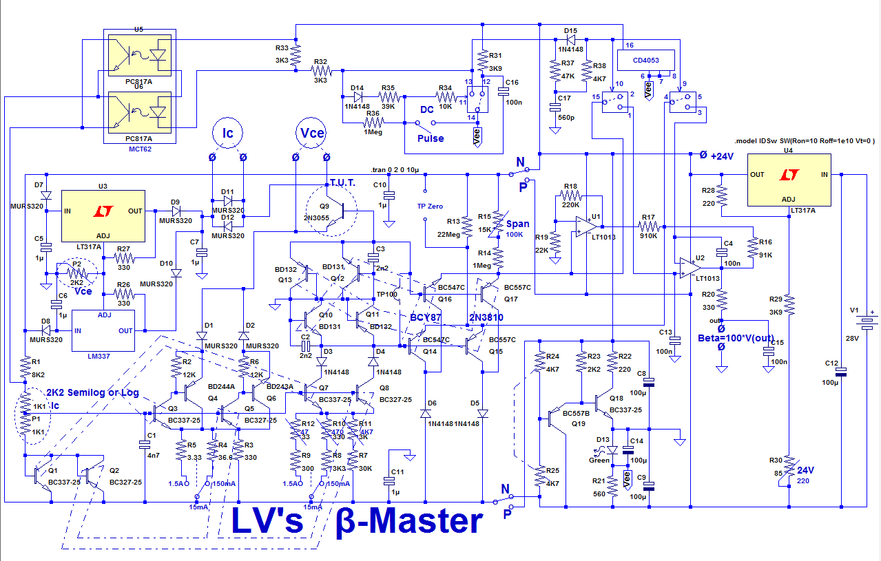
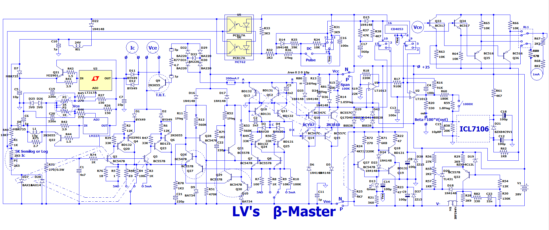
This is the circuit:
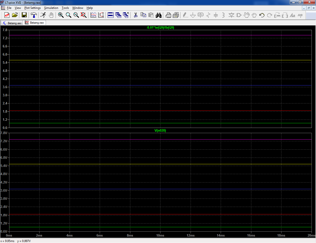
And a sim showing the measured value against the actual value (β+1 because what is actually measured is the ratio of Ie to Ib, not Ic/Ib):
https://www.diyaudio.com/forums/sol...collector-current-hfe-tester-transistors.html
The circuit proposed proved too complex for the OP, but I decided to bring it to completion anyway: it is probably a useful piece of kit for many DIYers.
The complexity, especially in its finished form, might look daunting, but that's kind of inevitable with this type of instrument: many parameters need to be made variable, and being a transistor tester, it has to accommodate both sexes, which brings another layer of complexity.
That said, the complexity is relative, and no expensive component is required.
It can be built as a naked board, with an external supply and multimeters as indicators, or as a complete, self-contained instrument (or anything in-between).
It does have some attractive features: it covers most of the needs for DIY use, with an Ic range of ~150µA to 1.5A, a Vce of 0 to 10V, requires a single unipolar supply, and the switches for the range and polarity are ordinary DPDT types (one has a center OFF).
A constant Ic tester is very convenient compared to alternatives improvised with supplies for example: comparisons are immediate and straightforward.
The direct-reading is also very convenient.
I didn't build and test a complete instrument: I just breadboarded the functional core for NPN (which operated as expected), and I also tested critical sections, like the polarity handling meaning the project is relatively safe.
The complete instrument has been tested in sim, and is functional (I include the .asc).
Note that this is a DIY-grade instrument, not a lab reference, but with care in construction and a good calibration, it is OK for a +/-1% accuracy, which is ample for a parameter like β.
Comparisons can be made with a greater accuracy.
This is the circuit:
And a sim showing the measured value against the actual value (β+1 because what is actually measured is the ratio of Ie to Ib, not Ic/Ib):
Attachments
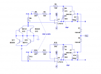
Here is a short description of the circuit:
The test current is generated by variable CCS's built around Q3 to Q6. The current feeds the emitter of the TUT, because it is more convenient than the collector, but in general, it will rarely matter: the displayed value will be β+1 rather than β, which makes practically no difference, except if the β value is exceptionally low, in which case one just needs to subtract one to the result, something that does not require an exceptional mental agility.
I have opted 15mA - 150mA -1.5A full scale, but it is perfectly possible to chose other values, or use a single range.
The Vce is also variable, and has its dedicated regulators.
The resulting base current of the TUT is converted to log thanks to Q12/13 and in parallel, a scaled image of the emitter current is logged by Q10/11.
The chosen scaling factor is 100, because it is a good median value for the β of ordinary transistors: it allows the logging transistors to operate at ~comparable current densities, which is desirable for a good accuracy.
The difference between the two log values is then converted by the differential antilog converter Q14->17 and U2. The converter is not fully balanced: the real antilog work is performed by Q16/Q17 only, with the rest providing compensation.
Taking the difference of two log values is equivalent to the quotient of the initial values, but the scale of the output needs to be referenced somewhere.
R14/15 with the 12V supply set the output at 1V when the log difference is zero, ie when the β of the TUT is 100.
The circuit can be calibrated by shorting TP100 and adjusting R15 (something I forgot to do in the sim, which is why the measured values are slightly too low).
There is no output offset adjustment, because offset errors are converted to span by the antilog circuit, meaning the span adjustment is theoretically sufficient to compensate all errors.
Theory and practice are somewhat different though, and precautions and corrections are required: the differential antilog converter has a single output, but it is not really single ended: its output is polluted by the log common-mode of the input.
The voltage is small, in the tens of mV, but it will degrade the accuracy especially for low β values.
U1 measures the CM wrt. ground and corrects the output of U2.
Internal errors cannot be corrected, which is why a precision opamp is required for U2.
The supply is a good, accurate 24V which is necessary because the supply voltage directly impacts the output.
Q18/19 split this supply to provide a low-impedance local ground.
If the supply source is an accurate, stable 24V, U4 can be omitted.
")
I hope so, now some practical considerations:
If the β-meter is built exactly according to the example, it will need (and thus dissipate) a significant amount of power: in excess of ~40W.
Some of that power will go into the voltage regulators, another part will be handled by the CCS and its emitter resistor, and finally the TUT itself will heat up considerably: at the max Vce-Ic, this would be 15W.
Substantial heatsinking is thus required, including for the TUT, perhaps especiallly for the TUT: even if it tolerates 150°C Tj, it is preferable to attach it to an ~infinite heatsink.
No need for huge extrusions or liquid cooling: the thermal resistance needs to be ~zero just for the time needed to make the measurement, a few seconds at most.
This means that a copper or aluminum block sufficiently massive can present a sufficiently low thermal impedance short term to make valid measurements.
Pulsed measurements are another option, and the βmeter could easily be modified to operate at a low duty-cycle. A µcontroller would be the logical choice to implement that, but two or three common analog circuits could do it as easily.
I may publish an extension later.
On the schematic, the dotted lines indicate the matching/thermal tracking relationships, and there are a number of them!
To attain the advertised performance, it is essential to respect these pairings.
The input transistors of the CCS's and their compensation have to be selected and matched, and in thermal contact, but well clear of the rest of the CCS: the emitter resistors and the power transistors.
The logging transistors Q11/13 and Q10/12 have to be carefully matched, and mounted in close thermal contact to ensure a proper, offset-free balance.
Q14 to Q17 being duals, they are inherently matched, but they need to be in thermal contact with the logging transistors, to cancel the effect of kT/q, the thermal voltage.
As a consequence, it is probably simpler to attach Q10 to Q17 to the same chunk of copper or aluminum: the collectors are common and grounded, and dual transistors have an isolated case.
R24 and R25 define the internal ground, and should be well matched because the resulting 12V is used as a reference.
It is important to remember that the output voltage representing β becomes negative for PNP transistors: with digital displays, that is not a problem, but if an analogue meter is used, the polarity switch will also have to reverse it.
I have developed the pulse extension, but first here is the corrected DC version, tweaked and calibrated (virtually) in .asc.
This shows the operation of the pulse extension, but behaviorally only: I don't have models for the CD4053.
I also include the .asc (BetamgP)
This is the physical circuit, based on the CD4053:
One of the operators is wired as an oscillator and the two other freeze the value on the output amplifier when the circuit is idle.
The dual optocoupler inhibits the CCS's during the inactive phase.
The frequency of operation is around 10Hz, and the duty-cycle is <4%, meaning a maximum dissipation in the TUT reduced from 15W to a little more than 0.5W.
I have used optocouplers, because the circuit needs to work for both polarities (and I was a bit tired and lacking inspiration).
A switch allows pulsed or DC operation; DC mode makes the Ic measurement easier.
The circuit has not been tested as a whole, but each function-block was.
Attachments
Miscellaneous...
Calibration:
The total supply voltage has to be 24.0V. Connect a voltmeter between the 24V TP and the (-) of the input supply; adjust R30 to read 24V.
The ratio of the output current to scaled current should be exactly 100.
Position P1 halfway, and for each current range measure the collector current by connecting an an ammeter between the E and C terminals of the tester.
Connect another ammeter across Q10 or Q11, and adjust R10->12 to read exactly 1/100 of the collector value.
With an ordinary transistor inserted, 150mA range P1 halfway, short TP100 and adjust R15 to read 1.000V at the output.
To check that all offsets (transistors, opamp) are under control, R13 can be replaced or paralleled to arrive exactly at the value of R14 + R15 (great accuracy is required) (TP100 still shorted).
The value at the output should not exceed +/-2~3 points of β (1point = 10mV).
If it is larger, there is a problem with the matching of the dual transistors or the offset of the opamp.
Resilience to miswiring, wrong polarities, etc.
The tester itself will tolerate any insertion or polarity error, or defective TUT without failure, and will protect the TUT for some situations, but not all.
I am not going to examine each case, but just an example: even a good transistor, of the correct polarity and correctly connected can be destroyed: if you test a BC547 at Ic=1A Vce=10V, it will be fried instantly.
There are many more ways of frying a good transistor, and there is no protection for that, except care and attention: you should always double-check the connection and settings before firing up the tester
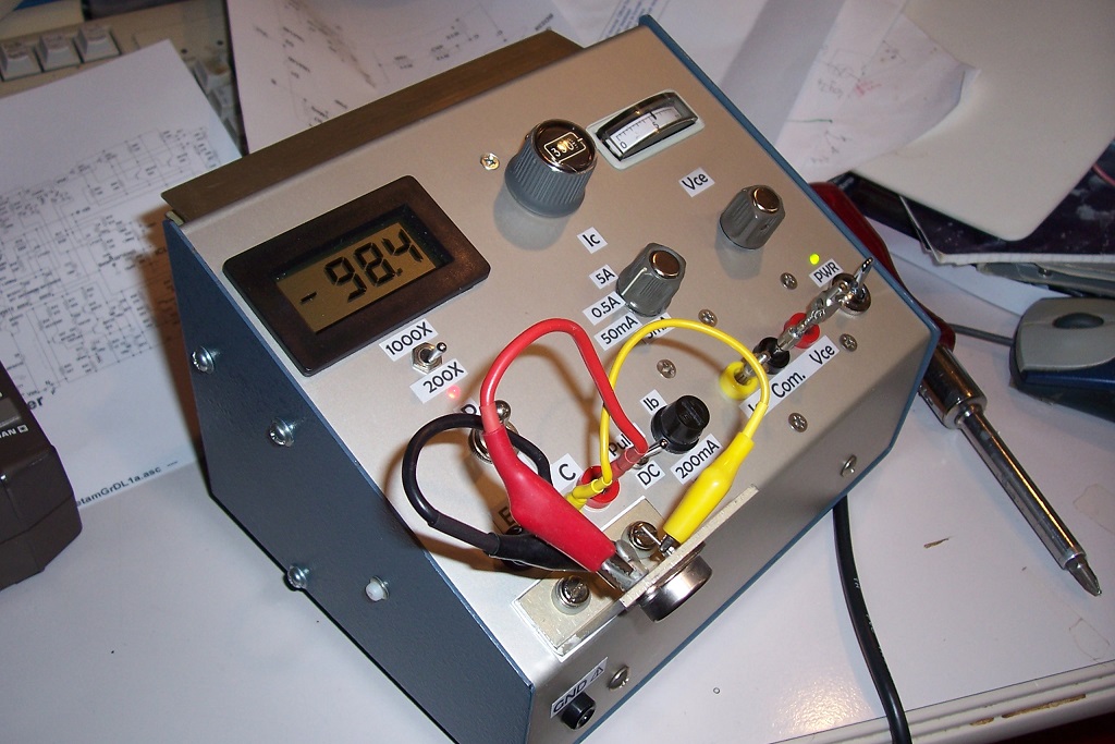
After many twists, delays and mishaps, I finally managed to build the "senior" version of this tester.
It has a higher maximum collector current, a total current range increased by two decades, increased accuracy, a pulse mode and permanently displays all the parameters.
It is an old-style instrument, with physical controls and displays and no "smart" functions, like automatisms or data export facilities.
It is thus perfectly suited for DIY and workshop use: testing a transistor takes a matter of seconds.
This is the main section:
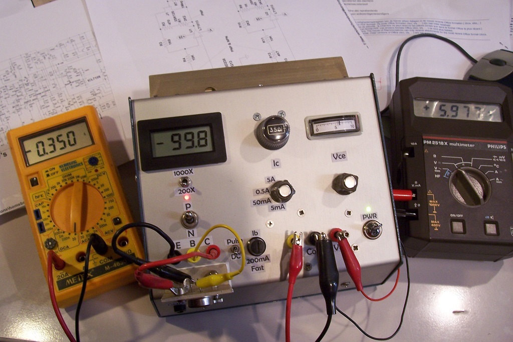
The instrument:
From the schematic the complexity looks daunting, but looking at the physical implementation the impression is somewhat different:

It has a higher maximum collector current, a total current range increased by two decades, increased accuracy, a pulse mode and permanently displays all the parameters.
It is an old-style instrument, with physical controls and displays and no "smart" functions, like automatisms or data export facilities.
It is thus perfectly suited for DIY and workshop use: testing a transistor takes a matter of seconds.
This is the main section:
The instrument:
From the schematic the complexity looks daunting, but looking at the physical implementation the impression is somewhat different:
Attachments

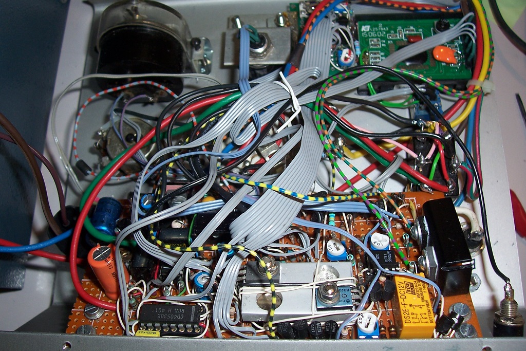
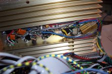
A close-up on the main section, part of the front-panel:
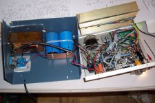
This is the power supply; extremely basic:
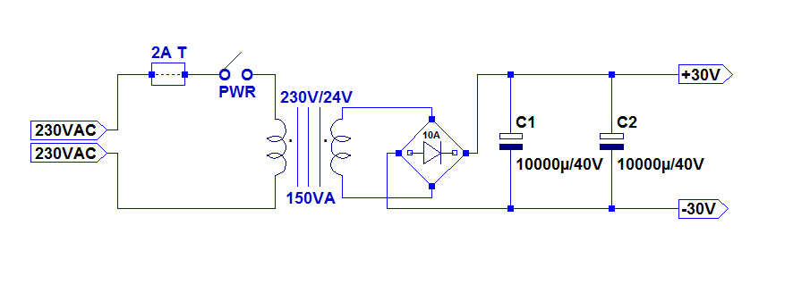
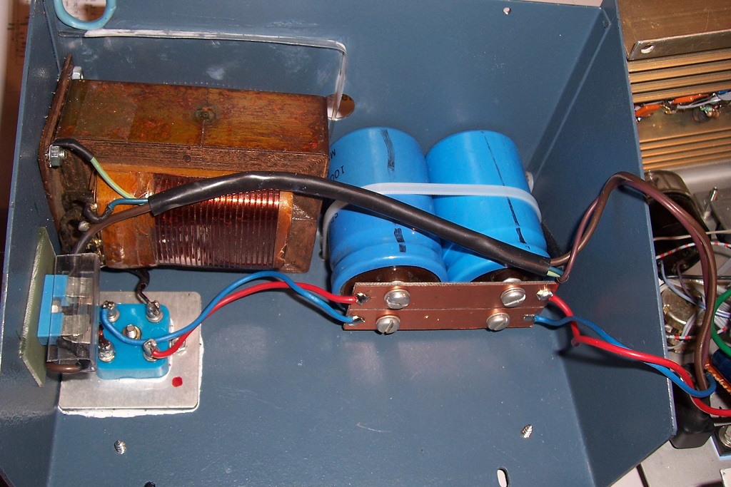
The transformer was pulled from an old slide-projector, probably 125 to 150VA with forced cooling. It is thus vastly under-dimensioned to provide a 5A DC output, but tests at this current level will be rare, and the thermal inertia is sufficient to make a number of consecutive tests without risking overheating.
Anyway, the main heatsink is similarly under-dimensioned, for the same reasons.
This is the correction board:
Later, I will explain why I had to add it
This is the power supply; extremely basic:
The transformer was pulled from an old slide-projector, probably 125 to 150VA with forced cooling. It is thus vastly under-dimensioned to provide a 5A DC output, but tests at this current level will be rare, and the thermal inertia is sufficient to make a number of consecutive tests without risking overheating.
Anyway, the main heatsink is similarly under-dimensioned, for the same reasons.
This is the correction board:
Later, I will explain why I had to add it
Attachments


Compared to the earlier, lighter version this one has a number of modifications and additions.
Many of them cope with the increased current and span, some result from the confrontation with reality, others were corrections of material errors, and finally I adapted the BOM to be able to use exclusively components from my stock.
The Vce regulators are now boosted, and have their outputs directly connected together.
I had to split the voltage-control potentiometer and add protection resistors R45 R46 to handle the opposite polarity.
The output voltage is also shifted ~3.6V by D25 & D26, to increase the Vce headroom.
The general supply needs to be split very accurately in 2, to ensure a perfectly symetrical operation for PNP and NPN, but this leaves too much headroom for the Ic regulators, and too little for the Vce regulators.
D25/26 and D29 to D33 address that issue.
I had difficulties stabilizing the boosted negative regulator. It is certainly not a configuration I would recommend, as the LM337 is a stinker.
In the end, I had to use 10µ ceramic bypass caps and an emitter-stopper choke for the boosting transistor.
It can also be made stable with just bypass caps, low-esr and >100µ, but this mandates Ecaps, and it isn't possible with this circuit, as it has to work for positive and negative voltages.
The main Ic current generator now uses triples, to manage the higher current and improve the accuracy.
It would be easy to achieve a good accuracy with an opamp, but it would be difficult with the constraint of the complete reversibility.
The slave Ic/100 generator is now based on CFP's, and tracks the main generator thanks to discrete quasi-opamps Q27 to Q31.
All of this allows the tester to work accurately for Ic settings < 1/100 of the nominal range.
This means 50µA for the 5mA range.
D27 & D28 are a better match for Q3 & Q5 than the transistors used initially.
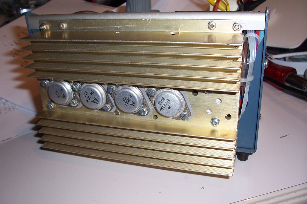
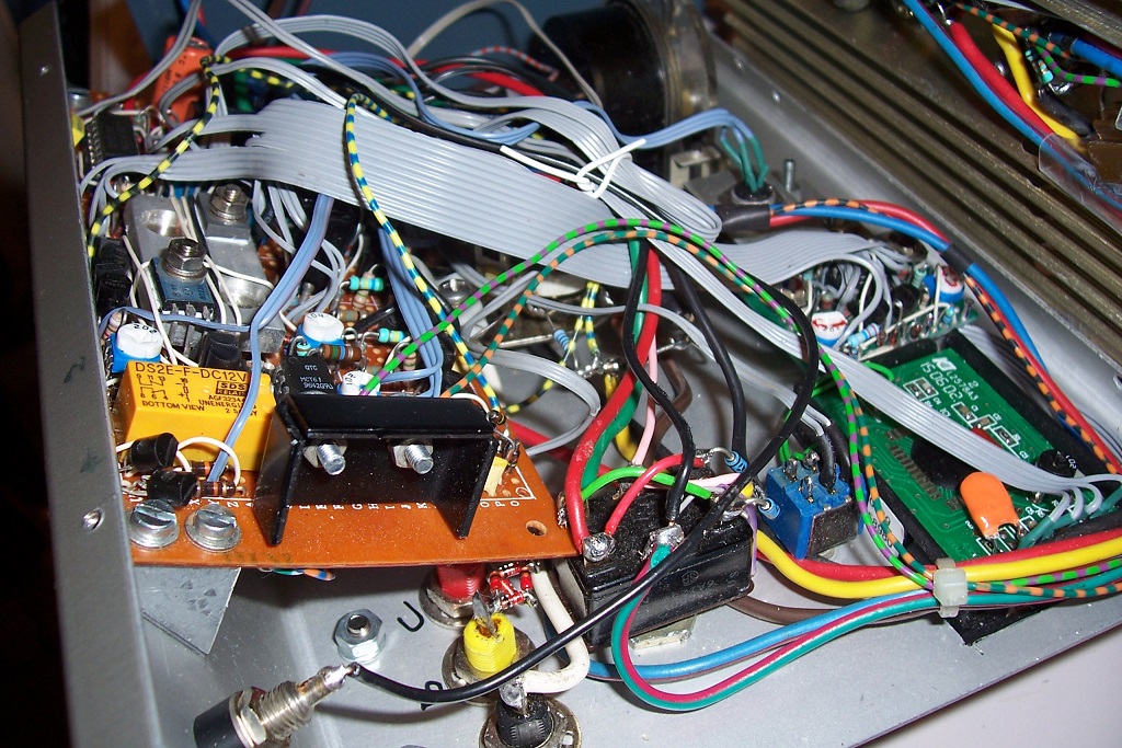
This the (well-populated!) main heatsink:

Another view of the innards:
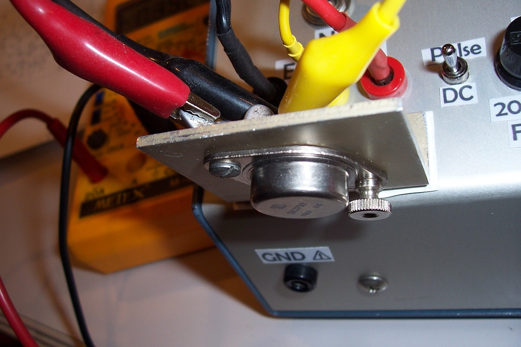
The front panel is fitted with an isolated fin, to easily test power transistors:
To be continued ...
Many of them cope with the increased current and span, some result from the confrontation with reality, others were corrections of material errors, and finally I adapted the BOM to be able to use exclusively components from my stock.
The Vce regulators are now boosted, and have their outputs directly connected together.
I had to split the voltage-control potentiometer and add protection resistors R45 R46 to handle the opposite polarity.
The output voltage is also shifted ~3.6V by D25 & D26, to increase the Vce headroom.
The general supply needs to be split very accurately in 2, to ensure a perfectly symetrical operation for PNP and NPN, but this leaves too much headroom for the Ic regulators, and too little for the Vce regulators.
D25/26 and D29 to D33 address that issue.
I had difficulties stabilizing the boosted negative regulator. It is certainly not a configuration I would recommend, as the LM337 is a stinker.
In the end, I had to use 10µ ceramic bypass caps and an emitter-stopper choke for the boosting transistor.
It can also be made stable with just bypass caps, low-esr and >100µ, but this mandates Ecaps, and it isn't possible with this circuit, as it has to work for positive and negative voltages.
The main Ic current generator now uses triples, to manage the higher current and improve the accuracy.
It would be easy to achieve a good accuracy with an opamp, but it would be difficult with the constraint of the complete reversibility.
The slave Ic/100 generator is now based on CFP's, and tracks the main generator thanks to discrete quasi-opamps Q27 to Q31.
All of this allows the tester to work accurately for Ic settings < 1/100 of the nominal range.
This means 50µA for the 5mA range.
D27 & D28 are a better match for Q3 & Q5 than the transistors used initially.
This the (well-populated!) main heatsink:
Another view of the innards:
The front panel is fitted with an isolated fin, to easily test power transistors:
To be continued ...
Attachments


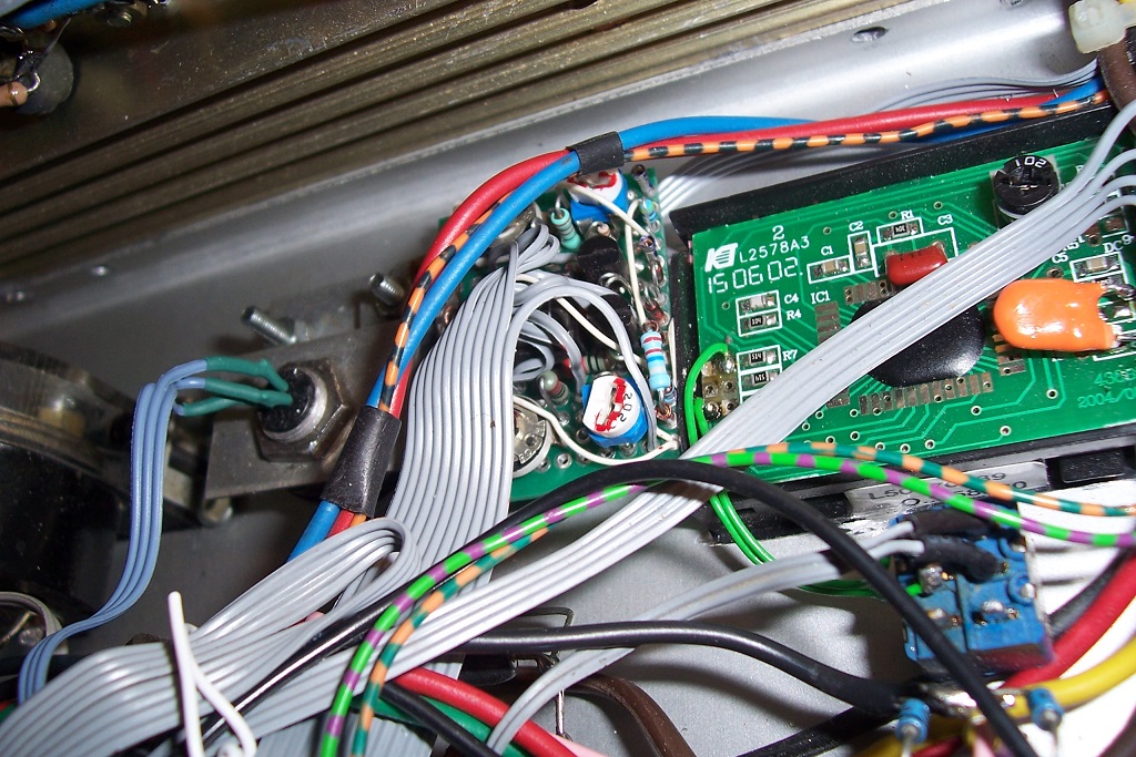
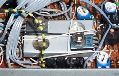
Most of the computing core engine has remained the same. As can be seen on the pic, all of the 8 transistors are attached to a single aluminum block, to ensure a perfect thermal tracking between the logging/anti log converters, and eliminate temperature gradients.

The base connection to the TUT has a stopper resistor and two ferrite beads in addition to the fuse and the voltage-shifting diode network.
They are necessary, because a transistor biased in linear regime and connected with loose cables can very easily oscillate.
The resistor and the fuse protect the TUT and the internal GND splitter against incorrect connections, or a faulty TUT (B-C short or collector connection open).
The antilog generator now include differentiated span and linearity corrections according to the N and P polarity of the TUT, thanks to D34,35 & 36.
The main 25V regulator is now discrete, because the transformer I used didn't supply enough voltage for a traditional VR when loaded with 5A.
The regulator built around M1 has an ultra-low dropout of <150mV @5A.
The instrument is now fully stand-alone, and includes a permanent display for Vce, Ic, and β.
The Vce indicator is a customized galvanometer, and includes buffer darlington transistors to avoid loading the measurement + a relay to adapt to the N and P polarity.
The β indicator is just a cheap LCD DPM with its supply and input divider.
The Ic indication is implicit: I used a multiturn potentiometer with a vernier/counter indication. It remains reasonably accurate down to 1/100th of the nominal range value, 50µA for 5mA.
In case better accuracy is needed, binding posts allow the transparent connection of external instruments:
Attachments

Initially, I had the hope to keep errors within a [+/-1% +/-1point] band.
I didn't know whether it would be achievable or not, but when I started the tests, my hopes were dashed: unexpected non-linearities appeared, and more importantly, the higher current ranges were affected by severe errors.
I analyzed the problems, and found that the linearity correction needed to be adapted, and polarity-dependent.
The complementarity between the logging and anti-logging transistors is imperfect, probably because they have opposite polarities, something I opted for to be able to attach all the logging transistors to a common block, with all the collectors at the GND potential.
The fix was easy: separate the correction resistors R13, R80 with diodes.
The high-current issue was more difficult: it was caused by the parasitic resistances of the logging transistors, mainly Re and Rb since Rc is practically cancelled due to the diode-connection.
With the initial, smaller project, I had a look at the spice parameters of the logging transistors, and they looked good enough without compensation.
This assumption was wrong from the start, and it was made worse with the higher current and better accuracy of this version.
The solution was to compensate these parasitic resistances. It could have been done by the transistors themselves, with a resistor in the collector, but with all collectors tied to GND, this was not an option.
I had to add the correction board: it senses the currents through R6 and R13, and adds an inverted correction to the voltage sent to the loggers.
Of course the PNP and NPN transistors have different parasitics and require a different correction.
This is achieved by the two switching FETs.
Unfortunately, this band-aid style of correction greatly complicates the calibration, as some adjustments act for both polarities, with an addition for the P only.
Added to the other polarity-dependent adjustements, it makes the calibration process a long and tortuous maze.
A V-2.0 could rationalize all that very easily, and do away with the needless complications, but I don't need another one, and I'll live with: after all, it remains calibrable, even if it is a PITA to carry out.
In the end, I couldn't remain exactly within the initial error envelope, but it was very close, with just a small violation for the 0.5A range.
It is probably possible to spread the errors differently, by adopting a different calibration strategy, and remain inside the envelope, but I didn't think it was worth bothering with it: the accuracy is already overkill for most cases, and comparisons, for matching purposes for example are almost perfectly accurate
Virtual ground:
The virtual ground is the result of unhappy tradeoffs.
It is an essential part of the circuit, and needs to be accurate and stiff, but if it is too inflexible, it will cause damages in case of wrong connections, or a defective TUT.
For example, if the collector of the DUT is open or disconnected, all of the emitter current will pass through the base, and thus the GND.
If the Ic is set to the maximum of 5A, it is a quite substantial current to handle, even if the base bonding wire withstands the treatment.
If the B and C are shorted, the GND will be directly shorted to the Vce supply, not very desirable either.
For these reasons, there are a number of protection/ mitigation mechanisms:
-a limiting 4.7ohm resistor and a fuse are inserted in the base connection
-the transistors Q18 and 19 have a limiting resistor in their collector
-Transils are installed between the GND and V+, V-; they are required to keep the CD4053 safe if the GND voltage wanders too far.
These are half-measures, and they limit the base current to 200mA, meaning it is not possible to test a Hfe lower than 25 at the 5A maximum collector current.
These arrangements aren't very satisfactory, but they work.
The main 25V regulator:
The general 25V regulator was made necessary because the transformer didn't have enough oomph to deliver 28VDC@/5A.
It is a completely ordinary, semidiscrete LDO and does its job perfectly.
The pulse mode
I had apprehensions about the pulse mode, but it is the one thing that worked absolutely spotlessly from the very start.
I took great care to design it as well as I could, fearing problems, and doing my homework paid: the pulse mode is perfectly transparent and works as well as is possible.
At low power levels, no difference is discernible between the pulse and DC modes.
At medium power levels, with the TUT in free air, when the pulse mode is activated, you see the beta dropping progressively as the transistor cools down.
Switching to DC has the opposite effect.
With a really high power, and the TUT attached to a heatsink, this behaviour is still present, but in addition there is an instantaneous gain change when the mode is switched: it is caused by the thermal resistance between the die and its surroundings.
As the thermal inertia of the die is tiny, the temperature (and beta) change appears instantaneous.
It can give interesting insights into the quality of the die to heat-spreader attachment..
Basically, the pulse mode only applies the test current during a very short proportion of the time.
The oscillator is an operator of the CD4053, and it controls the collector current through two optocouplers. It also controls the two other switches, operating as sample-hold for pulse mode, and low-pass filters for the DC mode.
Polarity control:
Since I have used an analog voltmeter for the Vce indication, I had to include a polarity inversion switch in the form of a relay.
Small darlingtons buffer the voltage, to avoid the burden of the voltmeter on very low Ic levels
For the record, here is the calibration procedure for this version:
Before starting, make sure the circuit is debugged, and seems to work consistently, even if the absolute values are off.
1-Adjust R55 to read 25.00V between V- and +25V
2-Check that the GND potential is 12.50V above V-. If a deviation is present, correct the 220K in // with R24.
3-Configure the settings to PNP, Vce=5V, range 50mA Ic=50mA and insert a general-purpose, medium-power transistor like BC327, 2N2905 or similar with a milliammeter in its collector lead. Make sure that the connections do not cause VHF oscillations in the transistor. If oscillations are present, fit a ferrite bead (~1µH) to one of the leads, generally the emitter, but sometimes the base and/or the collector.
Adjust R1 to read 50.00mA.
4-Disconnect the base from the test terminal and connect it to GND via a 10ohm WW resistor.
5-Using an external supply and a limiting resistor, inject a positive 300µA current into the base from the GND. Set Ic=30mA.
6-Adjust R15 to read a β of 101.0.
7-Switch to NPN; insert a medium-power NPN (BC337, 2N2219, ..). Reverse the auxiliary supply. Select a R51 value yielding a β reading of 101.0.
8-Adjust the aux supply to inject a base current of 149.25µA. Note the β reading, call it βH.
9-Set Ib at 1.5mA. Note βL. If βH/βL is >200/21, increase R80 and decrease it if βH/βL<200/21.Continue correcting R80 and redo steps 8-9 until βH/βL=200/21
10-Set Ib at 300µA and correct R51 to read 101.0
11-Insert a power NPN (with heatsink), switch to 5A, set Ic=3A, inject Ib=14.925mA.
Adjust R12 of the correction board to read β=200 (199.9 in practice)
12-Set Ib at 150mA and adjust R5 (correction board) to read β=21.0
13-Go through steps 7-12 as many times as required to obtain stable results.
14-Switch back to PNP, range 50mA Ic=30mA, auxiliary supply positive
15-Set Ib at 149.25µA; read βH
16-Set Ib at 1.5mA: read βL. If βH/βL>200/21 increase R13 and vice-versa.
Redo until βH/βL=200/21.
17-Set Ib at 149.25µA and check that β=199.9. If not, readjust R15
18-With a power PNP, range 5A, Ic=3A Ib=14.925mA, adjust R8 (corr.board) to read β=199.9
19-Set Ib at 150mA and adjust R1 (corr. board) to read β=21
20-Go through steps 14-19 until no changes are observed.
21-Redo steps 3-20 as many times as required to get stable results.
The procedure is obviously lengthy, laborious and iterative.
This is due to the "band aid" corrections interacting with each other and requiring many passes to eventually converge.
For this reason, I do not recommend duplicating exactly my build. It works, for sure, but is a PITA to calibrate.
The basic principles of the β-master are perfectly sound, and can be made to work, but the practical implementation should be amended to take into account the lessons learned from this first build.
The virtual ground, the Vce regulators and the protection of the TUT would benefit from a redesign
- Home
- Design & Build
- Equipment & Tools
- A constant-Ic β-tester: β-Master 🌈