OK, I understand your point. On the other hand I cannot imagine not having a laptop close to my bench to view datasheets and consult google.
Well, nothing prevents one from adding a capacitive touch 10" HDMI screen for 70 - 100USD and another RPi for 35USD into the digital section of the box, running REW without window decoration upon boot, respectively switching to a web browser with the DAC/ADC control using a regular toggle switch (simple to code in linux). If needed, the USB cable from the DAC/ADC board can be hooked to an external PC instead.
Well, nothing prevents one from adding a capacitive touch 10" HDMI screen for 70 - 100USD and another RPi for 35USD into the digital section of the box, running REW without window decoration upon boot, respectively switching to a web browser with the DAC/ADC control using a regular toggle switch (simple to code in linux). If needed, the USB cable from the DAC/ADC board can be hooked to an external PC instead.
Update. Attached is a photo of the ADC, 2 x ADS127L01. Preliminary measurements are right on target, -125dB THD @1KHz @48KHz sampling and is ruler flat (no noise shaping) up to the maximum sampling frequency, 384KHz. @20KHz THD is a measly -118dB @192KHz sampling.
Maximum sampling frequency is 384KHz with OSR=32. The secret for going that up (the max MCLK frequency is only 16MHz) is to take advantage of the internal slave/fsync mode, which includes double buffering. This makes possible to use a MCLK=12.288 MHz and BCLK=24.576MHz (both within the data sheet spec) with OSR=32. The 2 ADC chips are daisy chained. The on board logic (no CPLD or FPGA!) implements an addressable I2C bus, since in FSYNC mode the ADS127L01 internal registers are not accessible, so the external I2C bus controls directly the hardware pins. The board is still somehow experimental, lots of headers and jumpers are provided to facilitate measurements and various configurations. Converters are in slave mode, clocks are provided by a TI CDC925 synthesizer (in the future will come from the XMOS bosrd synthesizer). Board is fed by a single 5V (USB) voltage, everything (+/-12V for analog input stages, +3.3V digital, +3.3V analog, +2.5V reference) are generated on board by switching and linear low noise regulators. Reference is LTC6655 + LTC3045 and has about 5nV/rtHz (note to myself: need to measure again). Board is 4 layers with a solid ground plane split in 3, analog ground, digital ground and input analog stage ground, connected in single points to minimize the ground loops. Input stage is based on the THS4551 differential amplifier, with a switchable OPA827 single ended input. All passives RC are size 0602.
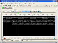
Attached is also a screenshot of the logic analyzer, with a few 384KHz conversion cycles, together with the serial conversion. Output is 32 bit, but bits 28-31 are always zero, while bits 24-27 are an internally generated checksum, which will be removed after transferring to the XMOS chipset.
Now, on to some serious and detailed measurements/characterization. I'll post the final measurements and the schematics if there is any interest.
Maximum sampling frequency is 384KHz with OSR=32. The secret for going that up (the max MCLK frequency is only 16MHz) is to take advantage of the internal slave/fsync mode, which includes double buffering. This makes possible to use a MCLK=12.288 MHz and BCLK=24.576MHz (both within the data sheet spec) with OSR=32. The 2 ADC chips are daisy chained. The on board logic (no CPLD or FPGA!) implements an addressable I2C bus, since in FSYNC mode the ADS127L01 internal registers are not accessible, so the external I2C bus controls directly the hardware pins. The board is still somehow experimental, lots of headers and jumpers are provided to facilitate measurements and various configurations. Converters are in slave mode, clocks are provided by a TI CDC925 synthesizer (in the future will come from the XMOS bosrd synthesizer). Board is fed by a single 5V (USB) voltage, everything (+/-12V for analog input stages, +3.3V digital, +3.3V analog, +2.5V reference) are generated on board by switching and linear low noise regulators. Reference is LTC6655 + LTC3045 and has about 5nV/rtHz (note to myself: need to measure again). Board is 4 layers with a solid ground plane split in 3, analog ground, digital ground and input analog stage ground, connected in single points to minimize the ground loops. Input stage is based on the THS4551 differential amplifier, with a switchable OPA827 single ended input. All passives RC are size 0602.
Attached is also a screenshot of the logic analyzer, with a few 384KHz conversion cycles, together with the serial conversion. Output is 32 bit, but bits 28-31 are always zero, while bits 24-27 are an internally generated checksum, which will be removed after transferring to the XMOS chipset.
Now, on to some serious and detailed measurements/characterization. I'll post the final measurements and the schematics if there is any interest.
Attachments
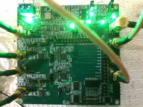
Update. Attached is a photo of the ADC, 2 x ADS127L01. Preliminary measurements are right on target, -125dB THD @1KHz @48KHz sampling and is ruler flat (no noise shaping) up to the maximum sampling frequency, 384KHz. @20KHz THD is a measly -118dB @192KHz sampling.
Maximum sampling frequency is 384KHz with OSR=32. The secret for going that up (the max MCLK frequency is only 16MHz) is to take advantage of the internal slave/fsync mode, which includes double buffering. This makes possible to use a MCLK=12.288 MHz and BCLK=24.576MHz (both within the data sheet spec) with OSR=32. The 2 ADC chips are daisy chained. The on board logic (no CPLD or FPGA!) implements an addressable I2C bus, since in FSYNC mode the ADS127L01 internal registers are not accessible, so the external I2C bus controls directly the hardware pins. The board is still somehow experimental, lots of headers and jumpers are provided to facilitate measurements and various configurations. Converters are in slave mode, clocks are provided by a TI CDC925 synthesizer (in the future will come from the XMOS bosrd synthesizer). Board is fed by a single 5V (USB) voltage, everything (+/-12V for analog input stages, +3.3V digital, +3.3V analog, +2.5V reference) are generated on board by switching and linear low noise regulators. Reference is LTC6655 + LTC3045 and has about 5nV/rtHz (note to myself: need to measure again). Board is 4 layers with a solid ground plane split in 3, analog ground, digital ground and input analog stage ground, connected in single points to minimize the ground loops. Input stage is based on the THS4551 differential amplifier, with a switchable OPA827 single ended input. All passives RC are size 0602.
Attached is also a screenshot of the logic analyzer, with a few 384KHz conversion cycles, together with the serial conversion. Output is 32 bit, but bits 28-31 are always zero, while bits 24-27 are an internally generated checksum, which will be removed after transferring to the XMOS chipset.
Now, on to some serious and detailed measurements/characterization. I'll post the final measurements and the schematics if there is any interest.
Schematics and Gerbers (even if just as a SMA test platform)! If what you have measured is repeatable and no other issues appear, many will ditch audio interfaces for measurements assuming it can adapted to a USB input device with a few more chips.
Now, on to some serious and detailed measurements/characterization. I'll post the final measurements and the schematics if there is any interest.
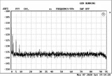
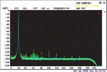
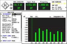
Not much time lately, unfortunately, but here's the noise floor: -138dB. Given the bib size of the FFT, this maps to a SNR of about -107dB, in line with the data sheet. Some spurious are due to the lack of shielding and my lab known contamination with 60Hz harmonics (see the LNA measurements discussion in another thread). No noise shaping effect, of course

Sampling rate is 192KHz, 2048 points FFT, MCLK=SCLK=12.288MHz, OSR=64, WB1 filter, ADS127L01 is in HR mode, differential inputs (THS4551 with gain=1) shorted, Vref=2.5V, channels are daisy chained.
Attachments
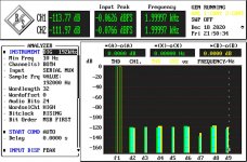
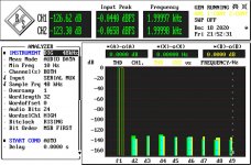
Distortions, see attached.
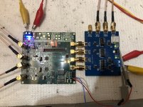
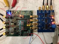
I build a simple synchronous clock divider (red board), 3 x 74LVC163 synchronous counters driven by a 24.576MHz 50ppm crystal oscillator plus three LMK1C1102 dual output clock drivers (one set of outputs for the ADC board, one set for driving the digital analyzer with SCLK, LRCK and SDOUT.
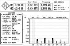
An ultra low noise 2KHz (<135dB) sine generator with balanced output is connected to both analog inputs, sampling frequency is 192KHz (I wish I could go to 384KHz, but my Rohde doesn't go that high).
Interesting asymmetry in THD, at -0.1dBFS. ADCs are sharing the same reference, so not much to look there. If I go down to -0.5dBFS the values balance nicely at around -120dB+/-1dB, which is what I was expecting at 192KHz. The delta at -0.1dBFS remains almost unchanged if I go down to 48KHz, or change the over sampling ratio (went down to MCLK=SCLK=3.072MHz and LRCK=48KHz), also balancing if I go to -0.5dBFS, to about -126dB. So it is either the THS4551 differential amplifiers at the input (I doubt) or something inside the ADC chips, I should bite the bullet and swap the two sets of chips, not much in the mood for this delicate surgery for now.
Anyway, another set of boards are on order, with better symmetry around the ADC chips and on board digital isolators from SiLabs. I cobbled a small board with 5+1 channels (3 clocks and 2 I2C lines, plus 1 SDOUT) and the noise decreases some 5 dB, bringing the ENOB to about 20.5dB which is again what I would expect. Right now, THD+N @192KHz is around -114dB, not too shabby, but I hope to bring it close to -120dB with the digital isolators.
I'll be back with more results.
I build a simple synchronous clock divider (red board), 3 x 74LVC163 synchronous counters driven by a 24.576MHz 50ppm crystal oscillator plus three LMK1C1102 dual output clock drivers (one set of outputs for the ADC board, one set for driving the digital analyzer with SCLK, LRCK and SDOUT.
An ultra low noise 2KHz (<135dB) sine generator with balanced output is connected to both analog inputs, sampling frequency is 192KHz (I wish I could go to 384KHz, but my Rohde doesn't go that high).
Interesting asymmetry in THD, at -0.1dBFS. ADCs are sharing the same reference, so not much to look there. If I go down to -0.5dBFS the values balance nicely at around -120dB+/-1dB, which is what I was expecting at 192KHz. The delta at -0.1dBFS remains almost unchanged if I go down to 48KHz, or change the over sampling ratio (went down to MCLK=SCLK=3.072MHz and LRCK=48KHz), also balancing if I go to -0.5dBFS, to about -126dB. So it is either the THS4551 differential amplifiers at the input (I doubt) or something inside the ADC chips, I should bite the bullet and swap the two sets of chips, not much in the mood for this delicate surgery for now.
Anyway, another set of boards are on order, with better symmetry around the ADC chips and on board digital isolators from SiLabs. I cobbled a small board with 5+1 channels (3 clocks and 2 I2C lines, plus 1 SDOUT) and the noise decreases some 5 dB, bringing the ENOB to about 20.5dB which is again what I would expect. Right now, THD+N @192KHz is around -114dB, not too shabby, but I hope to bring it close to -120dB with the digital isolators.
I'll be back with more results.
Attachments
ESS Technology :: Analog to Digital Converters
New from ESS.
A bit misleading in their marketing hype saying that the 128dB dynamic range, in mono mode, is the best on the market. It's not. The AK5578 will do 130dB in mono mode. Oh well ESS. At least you tried.
This is semantics mind you as a couple of dB is neither here nor there in the grand scheme of things.
Low distortion is promised, with a THD+N of -116/117dB, but without further information this is a little meaningless. If this were any other ADC manufacturer I'd expect it to mean at only 48kHz and at -1dBfs. With their DACs ESS has almost prided themselves on maintaining their THD specifications right across the range of sampling frequencies though (most likely because their DACs usually resample all incoming data to a high, fixed, sampling frequency) so who knows what this means.
As far as I'm concerned what I want to see is the THD vs input level for 48/96/192kHz. -1dB performance is great but if the THD falls back to -125dB by -8dB or so that would really be something to shout about. Even more so if it could do this at 192kHz.
Knowing ESS though getting this kind of information out of them is likely to be difficult. They are usually less than forthcoming with performance graphs but hopefully the datasheets and EVM literature will show us what we want to know.
There is no mention of the internal digital filters used, ie how flat they are and how the performance is maintained at higher sampling frequencies. But one nice caveat is that the ADCs come with a bank of biquads you can use in the digital data path. Even if the digital filters aren't perfect you could theoretically EQ the ADC to flat using its own internal processing.
Perhaps the biggest standout feature is the promised noise floor. Indeed the marketing blurb states an ultra low noise floor out to 200kHz.
Given the performance of ESS' last ADC I'm not exactly holding my breath. But given how much of a let down that was I'm sure ESS are somewhat aware that they can't fail again if they wish to be taken seriously, and have their ADCs widely adopted, by the professional market.
If this ADC does everything it says on the tin (plus the lower power consumption) it'll be quite the product. Maybe this will spur other manufacturers to produce something that can compete, AKM I'm mainly looking at you, but given the recent fire I can't see that happening for a while.
Edit - I was expecting these to cost a fortune but they are very reasonably priced.
Audiophile ADCs - Ismosys
Last edited:
Very, very hard to optimize this ADC, at all sampling rates and oversampling rates... My lack of experience in digital designs and the sad fact that a reference design for the ADS127L01 does not exist (the Texas Instruments EVM board is intended for showing the DC performance only, it does not include anything AC related) are certainly not helping...
I've found out the hard way (the data sheet is not exactly clear in this respect, only a short paragraph) that the ADS127L01 ADC inputs are not buffered, so the analog input signal conditioning requires quite some design and optimization, to avoid the switching glitches. Of course, the EVM input stage is not optimized for AC, although the required parts do have placeholders on the PCB.
Secondly, the required clocks for the Slave mode are tricky to set up; having MCLK, SCLK and LRCK synchronized (like for an audio ADC) leads to sub optimal results. For reasons I do not fully understand (and probably never will, given the lack of any insights of the chip internals) these clocks need a carefully timing between them and to the start of conversion (which here is on auto). I had to add RC cells on each clock lines and experimentally adjust each while optimizing for the overall distortion performance. Again the EVM has only a 10ohm/10pF RC on the MCLK line, which, as it is, does pretty much nothing to optimize the 3rd harmonic (that's where the impact is). Of course, I am talking here about <-100dB which is outside the scope of the EVM.
Here's the best results so far, still working on optimizing the beast. Needless to say that the PCB layout is also critical, I was not expecting having 2 chips to be so demanding in terms of symmetry and clocks distribution, after all it's only 12 MHz...
A digital 6 channel 5+1 isolator Si8661 was added to the PCB, and it helped a lot with breaking any ground loops. 3 inputs are the clocks, 2 inputs are the I2C lines and one output is the serial data out mux. The board in the photo has only the minimum circuitry soldered, the whistles and bells (power supplies for the high impedance input stage, the high impedance input stage (OPA827) allowing single ended input, the I2C expander) are set aside until the distortion performance is fully optimized.
The THD is now practically -120dB, which is what I was expecting. THD+N is now sligtly under -100dB, but from the spectrum it is clear that a big contribution is the spray of 60Hz harmonics up to 4-5KHz. In a shielded build, given the noise floor of under -140dB, I would expect a THD+N better than -110dB, which is again what I was expecting at this stage.
This is still work in progress, I want to get the last drop of performance out of this ADC. It is already better than any audio ADC I have seen, but it can do further down. I'll update here from time to time.
Attachments
Last edited:
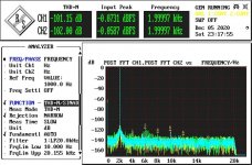
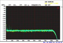
An averaged spectra clearly shows the harmonic (60Hz) noise being responsible for the THD+N performance. Hanning window, 8192 bins, 32 averages. Shielding is going to be required and it's not going to be trivial... With proper shielding I am now confident the THD and THD+N performances are going to be close, currently at about 0.0001% @2KHz/48KHz sampling.
Attachments
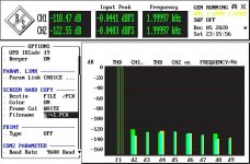
Follw up on post #307. This is the final version of the design and PCB. Same signal generator having 2KHz and THD about -129dB. At -0.1dBFS:
48KHz SR with oversampling x64, THD is -125dB.
192KHz SR with oversampling x64, THD is around -113dB.
This time the channels are almost perfectly symmetric. Providing an improved distribution for all clock signals and optimizing the timing (delaying the LRCK 4nS ref. MCLK and SCLK further delayed by some 3nS) pretty much cleaned the distortion spectra.
Noise floor is about -140dB with 8192 bins in 96KHz. Some spuriae are still visible, but nothing that I would not expect from an unshielded experimental board.
This concludes the experiments of using an industrial grade ADC for an audio analyzer, I am happy with the results, much better than I have seen with any audio grade ADC.
Now, on to the instrumentation DAC. Now that the AK4499 is on hiatus, the Rohm DAC not available yet for the unwashed masses, I have no idea what DAC chip would be the best for instrumentation. Thinking in going with the ESS PRO chip for the time being, eventually switching to the AKM stuff. The AK4499 chip is too expensive to experiment with, anyway. Remarkably, I cannot find any industrial grade DAC to compete with the best audio grade DACs.
Attachments
Now, on to the instrumentation DAC. Now that the AK4499 is on hiatus, the Rohm DAC not available yet for the unwashed masses, I have no idea what DAC chip would be the best for instrumentation. Thinking in going with the ESS PRO chip for the time being, eventually switching to the AKM stuff. The AK4499 chip is too expensive to experiment with, anyway. Remarkably, I cannot find any industrial grade DAC to compete with the best audio grade DACs.
Yeah, I think ES9028 or 9038 is probably your best bet. CS43198 could be worth a look also, but the performance is going to be a little lower and I think it is very focused on performance in the audio band and seems to have an earlier rise to the out-of-band noise. Plus the evaluation board is pretty expensive given what is on it.
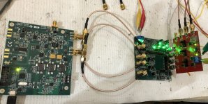
Below, 1KHz sine with THD -129dB sampled at 384KHz.
THD is -102dB (0.0008%), not too bad, about what I was hoping for. Unfortunately the digital analyzer doesn't let me include more than 10 harmonics, but I don't expect any sudden rise up to say 80KHz.
The DAC problem is still open... Apparently it is impossible to get an ES9038PRO evaluation board from ESS, wrote to a couple of companies that claim they can get one and got no resposes, could be only for recognized ESS partners? I designed an ES9038PRO DAC version with paralleling 4 channels, and an elaborate I/V stage, but since paralleling channels can be a two edged sword I would not dare creating a board before experimenting on a guinea pig like an eval board. Mistakes and errors would be too expensive, I can tell this from the ADS127L01 ADC development cycles, for which also no eval board allowing any serious AC evaluation exists.
CS43198, indeed the eval board is expensive (about half of the ES9038PRO board, though) for what's in, nothing that would help designing my own board, the bare minimum is in the eval board documentation (available for free), anyway.
The TI PCM1794, not good enough for instrumentation, IMO, and supports only 192KHz. After fighting the ADC to support 384KHz, limiting the sample rate in the DAC looks stupid to me. I'm hearing though that the actual PCM1794 performance is significantly better than the datasheet spec, maybe I should give it a shot... The 384KHz PCM5252 and the likes have only 114dB SNR, a vaste of time for instrumentation purposes.
So the DAC question is still open...
Attachments
- Home
- Design & Build
- Equipment & Tools
- ADCs and DACs for audio instrumentation applications