Hi Doug, 2nd version was almost done as a prototype 2 years ago, but because of a other projects, we did not finished the full firmware tests. There a a lot of features and a lot of various operation modes combinations, which equired a lot of time to test.
BTW, I got many questions this year bout it.
(Why this year? Why not 0.5y/1y or 1.5y ago? I don't know! Covid influence?") ).
).
So maybe I will force it now.
BTW, I got many questions this year bout it.
(Why this year? Why not 0.5y/1y or 1.5y ago? I don't know! Covid influence?
).So maybe I will force it now.
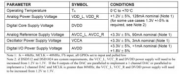
Can somebody tell from their own experience how much current is the ES9038PRO taking from:
+1.2V Analog (VDD_L, VDD_R)
+3.3V Analog Reference (AVCC_L, AVCC_R)
+1.2V Digital Core (DVDD)
+3.3V Digital I/O (AVDD)
+3.3V Oscillator (VCCA)
I am confused by the numbers in the data sheet (attached).
- Are these per channel (L/R) or the sum of currents on both channels?
- Why are VDD_L, VDD_R and DVDD collapsed under the same value, are they assuming one will use the 1.2V supply to feed both the Analog and Digital Core sections.
I read that the current value scale up (as expected) with the clock frequency, @100MHz and 768KHz is almost double the values @40MHz and 48KHz, anybody has any current consumption measurements @100MHz?
Attachments
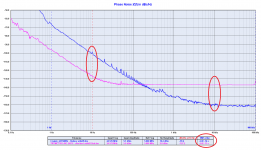
Not sure about audibility, but certainly the LF phase noise doesn’t contribute much to the jitter. That’s because the jitter is proportional to the square root of twice the phase noise integral, from zero to 2*fo. As such, usually the LF part of the phase noise area has a rather small contribution, in particular for frequencies fo in the tens of MHz, since the phase noise gets flat usually in the tens of KHz.
Maybe my instrument is broken?
Or I'm misunderstanding?
Attachments
You are both right. its all in how you measure jitter. And that can be a rabbithole since the connection between the different ways of looking at jitter : How to Measure Jitter << Microsemi. how those affect different signals in the output of a DAC (or input from an ADC) and how audible those effects are is still up for grabs. The only formal research I have seen suggests that this is all well under any audible threshold at least per AES: https://www.aes.org/tmpFiles/aessc/20210317/aes-12id-2020-i.pdf
I'm always for making something better if you know how and it doesn't bring too many problems. But there are absurd limits (Sapphire whispering gallery source? High-power solid-state sapphire whispering gallery mode maser - PubMed). And be careful of looking at a single issue when there could be other related aspects that affect what you are pursuing.
I'm always for making something better if you know how and it doesn't bring too many problems. But there are absurd limits (Sapphire whispering gallery source? High-power solid-state sapphire whispering gallery mode maser - PubMed). And be careful of looking at a single issue when there could be other related aspects that affect what you are pursuing.
If you start at 0.1 Hz and stop integrating at 100 kHz, sure. Perhaps you should work on improving your phase noise above 100 Hz rather than digging for a post you can score a point against.
You are wrong, the integration bandwidth starts at 10 Hz (the dashed red line).
So according to your science what would be the correct integration bandwidth to calculate the jitter?
12kHz to 100MHz suitable for telecommunication?
However you can also shift the integration bandwidth away from the carrier, the jitter will always be dominated by the phase noise closest to the carrier and not by the "flat" noise floor.
Try using a phase noise to jitter converter.
Lastly, the Pierce oscillator is followed by a couple of frequency doublers, so the noise floor inevitably increases.
Although the jitter is almost one order of magnitude better.
You are both right. its all in how you measure jitter. And that can be a rabbithole since the connection between the different ways of looking at jitter : How to Measure Jitter << Microsemi. how those affect different signals in the output of a DAC (or input from an ADC) and how audible those effects are is still up for grabs. The only formal research I have seen suggests that this is all well under any audible threshold at least per AES: https://www.aes.org/tmpFiles/aessc/20210317/aes-12id-2020-i.pdf
I'm always for making something better if you know how and it doesn't bring too many problems. But there are absurd limits (Sapphire whispering gallery source? High-power solid-state sapphire whispering gallery mode maser - PubMed). And be careful of looking at a single issue when there could be other related aspects that affect what you are pursuing.
Demian, I have not argued about the audible threshold of jitter, I got tired of this battle.
I merely wrote "my instrument is broken" if "usually the LF part of the phase noise area has a rather small contribution", because my instrument measures the opposite.
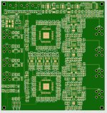
Ok, DAC is coming up... PCB (4 layers, 3.9"x3.7", top layer is shown, solid ground plane, power plane, routing plane) is in the final stage @JLCPCB, will get the boards next week. ES9038PRO are also coming from Mouser (they re-stocked the chips). PCB screenshot below.
- Top side row: +/-15V and +1.65V (LT3045 and LT3094) for the IV stages, plus the power sequencing circuitry (based on LTC2924)
- Top left corner, room for an 100MHz clock (the "horrible" Si570, I wonder about the difference between having both the ADC and the DAC synchronized, and having the DAC to run by it's own clock with high oversampling rate)
- Left column, digital inputs, SMA
- 2 ES9038PRO in mono mode.
- Mid row, analog power supplies, 3.3V, 1.2V based on the ADM7154 chips
- Left of the DAC chips, in a column, the digital power supplies, 3.3V, 1.2V, based on the LP5907 chips.
- Between the digital inputs and the power supplies, digital buffers and distribution, based on the LMK1C1102 chips.
- Right of the DAC chips, the I/V stages and reconstruction filters, 4 x OPA1622 (dials, for their high output current capability) plus 4x OPA1655 summing amplifiers.
- Right edge, analog differential outputs, SMA.
- Bottom left corner, more power digital power supplies (buffers, Si570 PLL, etc...) and the I2C interface connector (controls the DAC chips and the Si570).
Hope to have some measurements results in a couple of weeks... Then the XMOS digital integration and the input analog stages (with autoranging).
BTW, don't ask me how I learned, but the interesting schematic https://www.analog.com/media/en/technical-documentation/data-sheets/LT3094.pdf page 30 is on the bench a silicon graveyard. Both the LT8582 and the LT3045 are destroyed at the first power up, I've burned $100 in chips while experimenting. Still don't know exactly why it does this, but I assume is the missing P-Channel MOSFET on the positive rail. Per the LT8582 datasheet, this MOSFET allows the positive rail soft start, without this the LT8482 blows (since the control voltage from the LT3045 doesn't have a chance to settle and the converter is in full throttle until it would), and the spikes take out the LT3045 as well. It's a shame LT/AD pushed such an unverified (on the bench) schematic in the LT3094 data sheet.
Attachments
Last edited:
BTW, don't ask me how I learned, but the interesting schematic https://www.analog.com/media/en/technical-documentation/data-sheets/LT3094.pdf page 30 is on the bench a silicon graveyard. Both the LT8582 and the LT3045 are destroyed at the first power up, I've burned $100 in chips while experimenting. Still don't know exactly why it does this, but I assume is the missing P-Channel MOSFET on the positive rail. Per the LT8582 datasheet, this MOSFET allows the positive rail soft start, without this the LT8482 blows (since the control voltage from the LT3045 doesn't have a chance to settle and the converter is in full throttle until it would), and the spikes take out the LT3045 as well. It's a shame LT/AD pushed such an unverified (on the bench) schematic in the LT3094 data sheet.
This is quite surprising since AD has published some measurements and thermal images of the same dual power supply (Negative Linear Regulator Features 0.8 mV RMS Noise and 74 dB Power Supply Rejection Ratio at 1 MHz | Analog Devices). Maybe you should ask Molly for help
Actually anyone can order from ISMOsys and the price is per unit. I had 4 ES9822 Pro arrive this morning and they took about a week to get here from the date they were ordered. I too was surprised at how cost effective these ADCs are given their reputed performance.
Whether or not you are eligible to sign an NDA for the data sheets is another thing but that's up the people at ESS. It doesn't hurt to try. If you have a company email/name or website, of your own, you can go through that would make it easier.
I was surprised to see some of the ESS dacs turn up as mouser, including the data sheet and no NDA fuzz, they were just there to download. No adcs yet...
You can buy ADCs on the website Audiophile ADCs - Ismosys but is useless without the PDFs. I hope they were available soon.I was surprised to see some of the ESS dacs turn up as mouser, including the data sheet and no NDA fuzz, they were just there to download. No adcs yet...
ES9038PRO eval board appears to power DVDD, VDD_L, VDD_R all from the same regulator.
they are all connected internally, so no reason to do otherwise. check the notes after the pin descriptions table
Last edited:
Can somebody tell from their own experience how much current is the ES9038PRO taking from:
+1.2V Analog (VDD_L, VDD_R)
+3.3V Analog Reference (AVCC_L, AVCC_R)
+1.2V Digital Core (DVDD)
+3.3V Digital I/O (AVDD)
+3.3V Oscillator (VCCA)
I am confused by the numbers in the data sheet (attached).
- Are these per channel (L/R) or the sum of currents on both channels?
- Why are VDD_L, VDD_R and DVDD collapsed under the same value, are they assuming one will use the 1.2V supply to feed both the Analog and Digital Core sections.
I read that the current value scale up (as expected) with the clock frequency, @100MHz and 768KHz is almost double the values @40MHz and 48KHz, anybody has any current consumption measurements @100MHz?
they are total. I havent gotten as far along with the design as you, so i'm a ways off, although i'm about to order the chips at least and i'm working on my 9038q2m warm up. they have usually specified as total in their DS, although it's worded ambiguously.
as I mentioned. AVDD_L, AVDD_R and DVDD are all connected internally. I discovered that note, quite happily after doing a layout with separate regs for the AVDD, even 3 for those 3 pins, but it mentions they are all connected internally. That answers those pins. its specced for the 3 together.
regarding AVCC_L/R, if you take AVCC @ 3v3 * 0.924 = 3.0492 VPP, divided by the mono output impedance of 25Ω = 0.121968 * 1000 = 121.968mA output current, which is your 130 minus some margin, so it must be total for the dac.
Last edited:
They all run at the same voltage, but DVDD is a core logic digital power input. VDD_L and VDD_R are described as left and right analog power for the dac stage. Not finding where it says they are all connected together internally?
yes, its not well worded at all, if you dont catch the notes section near the bottom of page 5, you would think they are separate.
- Home
- Design & Build
- Equipment & Tools
- ADCs and DACs for audio instrumentation applications