While forgetting or not knowing that the ESS DAC actually works at a fixed x128 rate.
Last time I probed the output of ES9018 it changed state at every MCLK pulse (44.1k Fs, 45.1584 MHz MCLK) so maybe the DEM or the linear interpolator runs at MCLK but the digital filter runs at 128Fs?
IMO the DEM runs at MCLK and the ASRC resamples to MCLK/128. That would suggest why MCLK = 128Fs in the sync mode (no ASRC).
ES9038Q2M runs at full speed up to 768kHz - dirac pulse at 768kHz (128Fs MCLK 98MHz) https://www.diyaudio.com/forums/equ...-oversampling-filter-issue-8.html#post6661524
ES9038Q2M runs at full speed up to 768kHz - dirac pulse at 768kHz (128Fs MCLK 98MHz) https://www.diyaudio.com/forums/equ...-oversampling-filter-issue-8.html#post6661524
What do you mean by DEM - the actual thermometer decoding stage ie the actual DAC circuitry?
When looking at the output spectrum of an ESS board with a 100MHz clock with the FFT of our oscilloscope I noticed a spike at ~1.5MHz which would suggest to me the DAC runs at MCLK/64. Don't know for sure though.
EDIT: The DAC was running in asynchronous mode, datasheet here states that the minimum MCLK is 192FSR for asynchronous mode and 128FSR for synchronous mode. So the DAC output might run at MCLK/32 for synchronous mode - this is unconfirmed and just an educated guess though.
Last edited:
In ES9018 there's the 6-bit DAC itself, that makes 1LSB = 3.3/64 = 51mV steps which appears divided by 2 on below screenshot because 50R termination is on in the scope:

You can check at which frequency it runs by playing a low amplitude sine and looking for the max pulse frequency which occurs between two LSB levels. Since it is clocked by MCLK I doubt it runs at a multiple of Fs, most likely an integer division of MCLK.
I have a hunch that the hump may be due to the transition from multibit to 1 bit, which is why I suggested adding a 1/2 LSB digital offset to move this transition to another output level and see if that moves the hump. I can't test it because that board has been a victim of science
DEM is Dynamic Element Matching
Data is scrambled before being fed to the many 1-bit output cells. So if the 6 bit output value is, say, a string of 32 32 32, half of the cells will be on and half will be off, but they randomly swap places very fast, so in average, it is equivalent to all the cells being half-on half-off. This turns mismatch between cells into high frequency noise instead of distortion.
If this runs at MCLK that would explain why the output contains analog pulses at MCLK:

I'm not talking about the clock feedthrough spikes, I'm talking about the ~4mV pulse that repeats twice.
You can check at which frequency it runs by playing a low amplitude sine and looking for the max pulse frequency which occurs between two LSB levels. Since it is clocked by MCLK I doubt it runs at a multiple of Fs, most likely an integer division of MCLK.
I have a hunch that the hump may be due to the transition from multibit to 1 bit, which is why I suggested adding a 1/2 LSB digital offset to move this transition to another output level and see if that moves the hump. I can't test it because that board has been a victim of science
DEM is Dynamic Element Matching
Data is scrambled before being fed to the many 1-bit output cells. So if the 6 bit output value is, say, a string of 32 32 32, half of the cells will be on and half will be off, but they randomly swap places very fast, so in average, it is equivalent to all the cells being half-on half-off. This turns mismatch between cells into high frequency noise instead of distortion.
If this runs at MCLK that would explain why the output contains analog pulses at MCLK:
I'm not talking about the clock feedthrough spikes, I'm talking about the ~4mV pulse that repeats twice.
I have to admit now I'm confused
The second screen seems to show that the DAC outputs a bit every ~22ns or with a frequency of ~45MHz. What was your MCLK? Does this mean that the DAC changes values on all 64 resistors with a frequency of 45MHz? That would mean that the 6bit modulator is running at 45MHz which seems extremely fast IMO.
Or does it only switch voltage to one of the 64 resistors every 22ns?
Last edited:
I have to admin now I'm confused
Isn't it!
> The second screen seems to show that the DAC outputs a bit every ~22ns or with a frequency of ~45MHz. What was your MCLK?
Yes 45.1584M
> Does this mean that the DAC changes values on all 64 resistors with a frequency of 45MHz?
No because the height of the pulse is much smaller than one LSB which would be 1/64 of AVCC. Due to 50R scope termination it is double than what it says on the V/div, but that's still much lower than 1/64 AVCC.
I suspect the DEM/scrambling so the pulse would be mismatch between two output cells showing up. Or maybe it is leakage.
usually, 9822 both channels require the same or very close THD compensation but one of 6 units I prepared has one ch -129db another -135db(this is a typical level for all rest 5 units) 3rd harmonics, so, I have to quickly add to the FW an ability to use independent coefficients. And production test-application as well.
My measurements of ES9038Q2M right at the DAC pins in the sync mode (128Fs) have not shown any visible steps on the waveform:
https://www.diyaudio.com/forums/equ...-oversampling-filter-issue-7.html#post6661438 (scope just 1GSps)
https://www.diyaudio.com/forums/equ...-oversampling-filter-issue-8.html#post6662792
Wide BW analysis showed the first non-harmonic peak at MCLK (98.3MHz):
https://www.diyaudio.com/forums/equ...-oversampling-filter-issue-9.html#post6662805
That is my experience, others may have different results.
One more thing - to make the shown value on the oscilloscope amplitude half it's actual value the DAC's output impedance would have to be 50Ohm also - which DAC chip did you use? If it's the ES9018S that would mean all 8 outputs in parallel?!
To be honest, your guess is as good as mine: these measurements are from 5 years ago and there is a note that says "50 ohms termination - amplitude is wrong" but I don't remember how wrong
My measurements of ES9038Q2M right at the DAC pins in the sync mode (128Fs) have not shown any visible steps on the waveform:
If you do not see steps or pulses at the output of the DAC, then your DAC has an infinite number of bits, which is not possible. But if you are probing the output of the IV+filter and do not see any steps or pulses, it simply means your IV and output filter are doing an excellent job.
I don't remember how many bits 9038Q2M output DAC has, but you should test with a low digital amplitude signal to make the output pulse between two LSB levels, and probe at the output of the DAC, in voltage mode. If you probe with the IV connected and doing its job, it's a virtual ground, not much to see there.
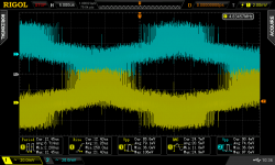
I've got this screenshot: ES9018 output, both channels in voltage mode, playing a sine wave at amplitude 1/64, Fs=44.1k
Attachments
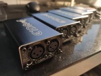
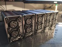
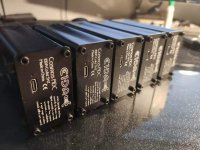
handmade samples for reviewers
Congratulations, but I believe this thread was intended to show designs of ADCs and DACs for instrumentation purposes, not simply for advertising commercial products.
So unless you are willing to share the schematics and perhaps the source code of your projects, IMO such messages do qualify as advertisement. There are special places on this forum that would gladly accommodate such messages, where the TI product team is announcing new audio related devices.
Your contributions with measurements and qualification of chips are appreciated and do fit here, thank you.
Last edited:
Of course we need those few extra dB:s of lowerTHD. Size of PCB is not important. It is what you can do with it that matters.
Will there be a PRO version (in a larger box with also better THD+-N)?
Will there be a PRO version (in a larger box with also better THD+-N)?
5 samples of Cosmos ADC were soldered by my hands and will be sent for tests.
Regarding compensation technics, no doubt does exist the way to get 9822 THD even better but who really needs that if a simple 90x50mm board being powered from USB, provides a few db better THD+N performance than AP SYS2***?
The initial idea was to design an ADC with UAC2 attenuator. I found a way to attenuate up to 10Vrms with THD-N <-130db and 600ohm impedance. I built 6 iterations of such ADC proto, and got pretty much the same DR/THD+N performance like the current Cosmos ADC version, simplified one. However, USB 5V rail consumption was nearly unacceptable high + about 4x times parts count makes Cosmos ADC Pro(let's call it that) noticeable more expensive. Finally, I decided to start with a simplified Cosmos ADC design with the same 8 steps attenuator with a DIP-switch instead of MOSFETs. The BOM cost dropped down, the performance slightly get's up, the design becomes a bit more viable(lower than standard 10k input impedance is the drawback).
Regarding a lower THD+N(if somebody still not happy with THD+N -123db!), technically it is possible with paralleling of multiple ADC chips, that involves a DSP, also a good idea to fit the same housing ADC+DAC together. However, I'm not really a company to take such risk and design so expensive device without demand investigation. So, Cosmos ADC is the first try.
Regarding a lower THD+N(if somebody still not happy with THD+N -123db!), technically it is possible with paralleling of multiple ADC chips, that involves a DSP, also a good idea to fit the same housing ADC+DAC together. However, I'm not really a company to take such risk and design so expensive device without demand investigation. So, Cosmos ADC is the first try.
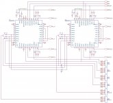
Schematics galore
Here are the schematics for the ES9822PRO ADC. It is dual mono, however the data sheet is unclear on how to set up multiplexing left/righ data on the same output. I had to make some assumptions and added switching bridges (resistors) to allow several possible combinations. Trial and error will follow...
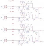
The input stage use the OPA1612 opamp, not much to comment about.
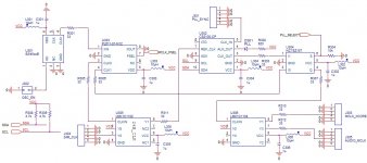
The power supply, I decided to use the ES9311 LDO regulators for the Reference voltages. The ES9822PRO data sheet is also unclear about the performance required in the AVCC power supplies, so I decided to assume the worse and throw in a pair of extra LT3045 (probably an overkill). Power sequencing is per the ES9822PRO data sheet.
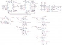
Also attached is the clock generator for the integration with the XMOS chip (software is in development). Pretty much the XMOS audio reference board implementation, with a few tweaks (added clock buffers and series resistors for clock distribution, used a decent clock chip instead of a simple crystal, modified the power distribution).
Unfortunately my Rohde UPD supports only the digital generator as a Master and the digital analyzer as a Slave. There are LRCK I/O BNCs on the back panel, but using those to recover the master clock would require an external ASRC. It would be great if the ES9038PRO DAC (in slave mode) could output the reconstructed x128 SR internal clock, to use it for clocking the (also in slave mode) ADC, unfortunately it doesn't. Or if the Rohde UPD would output the Master clock from the digital output, to be able to drive in sync both the DAC, the ADC and the Slave digital analyzer, unfortunately it also doesn't. So the only way I see possible to test the setup of the ADC and DAC at all SRs is to use the clock generator to drive the ADC and the DAC D_PLL in async mode.
After the XMOS board will be completed (hardware and software still in development) this will not be an issue, because both the DAC and the ADC will work in Slave mode.
Some parts may still have incorrect values, due to the heavy copy/paste when drawing, sorry about. Comments are welcomed, I am in particular interested in ideas for loop testing, before integrating with the XMOS controller and USB bridge.
Here are the schematics for the ES9822PRO ADC. It is dual mono, however the data sheet is unclear on how to set up multiplexing left/righ data on the same output. I had to make some assumptions and added switching bridges (resistors) to allow several possible combinations. Trial and error will follow...
The input stage use the OPA1612 opamp, not much to comment about.
The power supply, I decided to use the ES9311 LDO regulators for the Reference voltages. The ES9822PRO data sheet is also unclear about the performance required in the AVCC power supplies, so I decided to assume the worse and throw in a pair of extra LT3045 (probably an overkill). Power sequencing is per the ES9822PRO data sheet.
Also attached is the clock generator for the integration with the XMOS chip (software is in development). Pretty much the XMOS audio reference board implementation, with a few tweaks (added clock buffers and series resistors for clock distribution, used a decent clock chip instead of a simple crystal, modified the power distribution).
Unfortunately my Rohde UPD supports only the digital generator as a Master and the digital analyzer as a Slave. There are LRCK I/O BNCs on the back panel, but using those to recover the master clock would require an external ASRC. It would be great if the ES9038PRO DAC (in slave mode) could output the reconstructed x128 SR internal clock, to use it for clocking the (also in slave mode) ADC, unfortunately it doesn't. Or if the Rohde UPD would output the Master clock from the digital output, to be able to drive in sync both the DAC, the ADC and the Slave digital analyzer, unfortunately it also doesn't. So the only way I see possible to test the setup of the ADC and DAC at all SRs is to use the clock generator to drive the ADC and the DAC D_PLL in async mode.
After the XMOS board will be completed (hardware and software still in development) this will not be an issue, because both the DAC and the ADC will work in Slave mode.
Some parts may still have incorrect values, due to the heavy copy/paste when drawing, sorry about. Comments are welcomed, I am in particular interested in ideas for loop testing, before integrating with the XMOS controller and USB bridge.
Attachments
Last edited:
handmade samples for reviewers
May I review one?
And yes - either show the schemas or go -> commercial section...
//

- Home
- Design & Build
- Equipment & Tools
- ADCs and DACs for audio instrumentation applications