This stuff may give you some ideas for dividers: http://www.wriley.com/A High-Resolu...er Using the TAPR TADD-2 and TICC Modules.pdf These guys are at the bleeding edge on things like phase noise. The more common programmable dividers can have significant spurs which would degrade the floor.
These "may" be useful: https://www.idt.com/us/en/document/...st-edge-rate-and-low-phase-noise-requirements
I saw the fS jitter number which seems more than a little beyond reality not to mention way beyond anything that could be measured. I believe there is a more complex relationship between jitter and jitter spectrum and the sampling period and the frequency of the signal to be sampled. In effect all these are mixed together in various ways by the sampling process so there are interactions. Still all way below anything that will compromise performance. Actually getting a low jitter clock across a PCB is a serious and challenging task.
I don't know what options Virtins has, but I did find this paper that has nice descriptions of common functions and tradeoffs:
https://prod-ng.sandia.gov/techlib-noauth/access-control.cgi/2017/174042.pdf
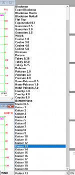
Here are the window options Virtins provides (the Kaiser go up to 20).
Any direction will be greatly appreciated.
Attachments
This stuff may give you some ideas for dividers: http://www.wriley.com/A High-Resolu...er Using the TAPR TADD-2 and TICC Modules.pdf These guys are at the bleeding edge on things like phase noise. The more common programmable dividers can have significant spurs which would degrade the floor.
These "may" be useful: https://www.idt.com/us/en/document/...st-edge-rate-and-low-phase-noise-requirements
I saw the fS jitter number which seems more than a little beyond reality not to mention way beyond anything that could be measured. I believe there is a more complex relationship between jitter and jitter spectrum and the sampling period and the frequency of the signal to be sampled. In effect all these are mixed together in various ways by the sampling process so there are interactions. Still all way below anything that will compromise performance. Actually getting a low jitter clock across a PCB is a serious and challenging task.
Thanks, never mind, I settled for and ordered some CDCE913 from TI. Not exactly my ideal, data sheet says max 100pS jitter for x1 output, I'll see what I can get out of it, after dividing for CNV (48KHz-768KHz) from a 24.576MHz. No, I don't want to use a DIR like AK4118, since I can't find any supporting over 192KHz.
Thanks, never mind, I settled for and ordered some CDCE913 from TI. Not exactly my ideal, data sheet says max 100pS jitter for x1 output, I'll see what I can get out of it, after dividing for CNV (48KHz-768KHz) from a 24.576MHz. No, I don't want to use a DIR like AK4118, since I can't find any supporting over 192KHz.
Will this work? I didn't get a chance to read the datasheet fully, but it might:
AD9508 Datasheet and Product Info | Analog Devices
Another option, which is probably a lot more work is to use a CPLD or tiny FPGA like a Lattice iCE40 and reclock the outputs. It has a free toolchain I believe.
Will this work? I didn't get a chance to read the datasheet fully, but it might:
AD9508 Datasheet and Product Info | Analog Devices
Another option, which is probably a lot more work is to use a CPLD or tiny FPGA like a Lattice iCE40 and reclock the outputs. It has a free toolchain I believe.
Thanks, I've seen it, the AD9508 is the next in line
") It is not easy for me to prototype with a LFCSP, so if the TI part fails I'll get this one. Otherwise, it looks too good for my modest target .
It is not easy for me to prototype with a LFCSP, so if the TI part fails I'll get this one. Otherwise, it looks too good for my modest target .CPLDs and FPGAs are always the universal answer, not a big fan, plus that my VHDL is rusty at best.
Well, with a standard 24.576MHz quartz, the x1 CDCE913 output has a phase noise of -125.8dBc flat, which is about 31pS jitter (better than the data sheet spec which is 60pS typ. 100pS max.). I'll measure the phase noise after division to 512 for the 48KHz LRCK (and CNV) clock, but it appears it is going to be fine.
Stay tuned, I am working on interfacing a 20bit SAR with my UPD Rohde analyzer, planning to follow this: http://www.ti.com/lit/an/slwa036/slwa036.pdf
Not expecting anything special (the SNR is already what I would expect from a practical 20 bit ADC) and, besides, there's not much to do about, since all these ADCs have an internal clock/PLL for conversion. The external clock is only for shifting out the data over the SDO.
So you must have the S/PDIF OPT AES/EBU options etc?
So you must have the S/PDIF OPT AES/EBU options etc?
I do.
I saw the fS jitter number which seems more than a little beyond reality not to mention way beyond anything that could be measured.
fs jitter times are routinely measured. You know phase noise and jitter are directly related?
RE =170 dBC When I was discussing getting a crystal oscillator from Wenzel they told me that to get an oscillator with that performance I would need to sign ITAR papers since that performance level was considered munitions grade and controlled. Further I would not be able to sell it outside the US without DOD approval.
However it seems those limits no longer apply.
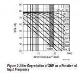
In any case its not quite that simple. first measuring less that 100 fS jitter directly is not really possible with available technology. You can measure the phase noise although measuring at -170 dBC its really difficult. Then you need to be sure what you are measuring it what matters. The chart below is for SAR type converters and shows the relationship between jitter and SNR vs. frequency. Maybe it would be useful to extrapolate the chart to audio frequencies and SNR's.
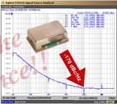
The other charts show the jitter analysis of the crystek CCHD-957 at 24 MHz. its an RMS jitter of around 300 fS and dominated buy the 10 Hz to 100 Hz block. What I have come to understand is that those lower frequencies have the least influence on SNR and audibility. I may well be simplifying it since the audio stuff is full of controversy and contention but the industrial stuff tends to be pretty clear.
However it seems those limits no longer apply.
In any case its not quite that simple. first measuring less that 100 fS jitter directly is not really possible with available technology. You can measure the phase noise although measuring at -170 dBC its really difficult. Then you need to be sure what you are measuring it what matters. The chart below is for SAR type converters and shows the relationship between jitter and SNR vs. frequency. Maybe it would be useful to extrapolate the chart to audio frequencies and SNR's.
The other charts show the jitter analysis of the crystek CCHD-957 at 24 MHz. its an RMS jitter of around 300 fS and dominated buy the 10 Hz to 100 Hz block. What I have come to understand is that those lower frequencies have the least influence on SNR and audibility. I may well be simplifying it since the audio stuff is full of controversy and contention but the industrial stuff tends to be pretty clear.
Attachments
What I have come to understand is that those lower frequencies have the least influence on SNR and audibility. I may well be simplifying it since the audio stuff is full of controversy and contention but the industrial stuff tends to be pretty clear.
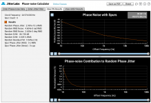
Not sure about audibility, but certainly the LF phase noise doesn’t contribute much to the jitter. That’s because the jitter is proportional to the square root of twice the phase noise integral, from zero to 2*fo. As such, usually the LF part of the phase noise area has a rather small contribution, in particular for frequencies fo in the tens of MHz, since the phase noise gets flat usually in the tens of KHz.
Last edited:
Not sure about audibility, but certainly the LF phase noise doesn’t contribute much to the jitter. That’s because the jitter is proportional to the square root of twice the phase noise integral, from zero to 2*fo. As such, usually the LF part of the phase noise area has a rather small contribution, in particular for frequencies fo in the tens of MHz, since the phase noise gets flat usually in the tens of KHz.
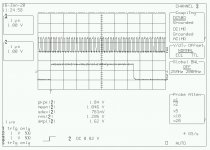
Ok, so the ADC clocking works to my satisfaction, using the CDCE913 clock generator. Feeding from a 24.576MHz ultra low jitter oscillator (Crystek CCHD-957-25-24.576) straight dividing by 32...512 for the LRCK (also the sampling clock), using the internal frac PLL to up the frequency by x8, x6, x5, x4, x2 then divide by 4, 8, 16, 32, 64 for the BCLK. All possible combination of 8, 16, 20, 24, 32 bit and 48, 96, 192, 384, 768 KHz sampling are available. A simple logic with a 74LVC04 hex inverter and a 74LVC02 quad NOR creates the CNV pulses (>20nS) on both LRCK edges (for two channels), so that the LTC2378-20 acquires the input and starts the conversion (completes in less than 675nS).
Clocks are clean and nicely synced, see below (32bit@768KHz sampling, 49.152MHz BCLK, I may eventually try a 32bit SAR, not a priority since I'm not expecting anything better compared to the 20bit LTC2378). The LRCK has a phase noise/jitter below what I can quickly and reliable measure and is certainly under 1pS.
Feeding the LTC2378-20 with these signals (CNV, BCLK) renders the target performance (THD<-125dB, SNR>103dB) expected from this SAR ADC.
I wonder if 44.1KHz ADC sampling is required for instrumentation purposes?
Attachments
Last edited:
I would provide for a 44.1 clock chain for several reasons-
1) Some unanticipated backward compatibility requirement
2) I like to measure 48 K devices with 44.1 clocks to ensure there are no hidden synchronous things happening
3) I believe those clocks have an enable pin so its pretty trivial to tie two XO's together and switch between them. No intervening logic required.
Far more important is making sure the clock performance isn't compromised in distributing it to the ADC. The original demo board for the AK5394A had a gate oscillator for the master clock on a shared chip and it had lots of issues. Using an external Crystek oscillator (and some other obvious fixes) got almost 20 dB improvement in spurs and distortion confirming to me how important those details are.
2) I like to measure 48 K devices with 44.1 clocks to ensure there are no hidden synchronous things happening
This is a very good point. Analogy - measurements are typically performed at 1kHz which is a major USB frequency.
44.1 is a bit more complicated to transfer over USB than direct multiples of 1kHz, it may take more work on the device firmware if being produced in-house.
I would provide for a 44.1 clock chain for several reasons-
1) Some unanticipated backward compatibility requirement
2) I like to measure 48 K devices with 44.1 clocks to ensure there are no hidden synchronous things happening
3) I believe those clocks have an enable pin so its pretty trivial to tie two XO's together and switch between them. No intervening logic required.
Far more important is making sure the clock performance isn't compromised in distributing it to the ADC. The original demo board for the AK5394A had a gate oscillator for the master clock on a shared chip and it had lots of issues. Using an external Crystek oscillator (and some other obvious fixes) got almost 20 dB improvement in spurs and distortion confirming to me how important those details are.
This is a very good point. Analogy - measurements are typically performed at 1kHz which is a major USB frequency.
44.1 is a bit more complicated to transfer over USB than direct multiples of 1kHz, it may take more work on the device firmware if being produced in-house.
Ok, this will need a second frac PLL, not a big deal, there is a CDCE925 with two PLLs, I'll take care of that. The LRCK and BCLK outputs will have to be gated with the main clock generator, also not a big deal. I'll come up with some results soon.
Ok, so I have to admit defeat on this topic and put it on the back burner, before even reaching the "project" status.
Recognizing that the current audio ADC chips are the toughest limitation for audio instrumentation purposes, I was looking into industrial grade ADCs and check if they would be more appropriate. I've explored the Analog Devices LTC2378-20 (20bit 1Msps SAR), the TI ADS8900 (20bit 1Msps SAR) and the TI ADS127L01 (24bit sigma delta, 500Kbps). All these chips met or exceeded what I think should be the acceptable limit for audio instrumentation purposes (sampling rate minimum 384KHz, noise floor better than -150dB up to 192KHz, THD better than about -125dB @2KHz and better than -115dB @20KHz, as much as possible independent of the input level, down to the harmonics in the noise floor) so the prospects were initially good. I also explored a few chips for generating a high quality clock tree (AD9508, CDCE913) with great results; 1pS or better jitter was not difficult to get with these modern chips.
Where I failed miserable was in the digital signal processing; I am by no means an professional electronics designer, and much less a professional digital electronics designer, but I am not scared of software/firmware development when/if I get to that; so I though the digital processing will be the least difficult issue to tackle; I couldn't be more wrong.
First, all these industrial grade ADC chips are outputting what the data sheet calls "SPI compatible" serial data. I thought "SPI compatible" means some resemblance to the SPI specification, and it does; the interface is 3 wire or 4 wire with chip select. However, now what? Passing SPI over an USB transport is doable (more about later) but what good would that make? I was not about to write a PC based spectrum analyzer that bypasses the USB 2.0 audio interface, or even less a set of drivers that would convert SPI with the I2S in the target OSs. So it would be more logical to convert SPI to I2S on the ADC side and leave the computer side work to be handled by the ASIO4ALL driver up to the PC application level. That's an much easier win, and it took only a few nights works to implement a SPI to I2S bidirectional bridge, using an Altera/Intel EPM1270 CPLD, even with my rather poor VHDL knowledge. To my surprise, there are more or less critical timing issues buried in the ADC chips data sheets that would not allow any obvious (to me) one-size-fits-all CPLD implementation (but I could be wrong, I don't know) so the VHDL code had to be slightly adjusted for each chip. So "ISP compatible" doesn't really mean "ISP spec compliant"...
Ok, then again, now what? I thought it's time to pass back and forth the I2S data over USB. And here's where the big shock came.
First, the I2S spec elaborated by Phillips in the 90's is low speed (up to 48KHz) only; the eventual extension to 192KHz elaborated by Cirrus (if memory serves) was largely ignored by the industry.
Secondly, the SPI protocol is addressable, including 8bit of command and only 16bit of data, so not a chance in hell to send 20/24bit data in a single frame over USB, a multiple frame approach is needed (which again is not rocket science to implement and could still use the existing USB 1.0 and/or USB 2.0 transport hardware/firmware). But with what impact in performance (except for latency that for instrumentation purposes could be ignored, or at least I think so)?
Third, with two exceptions, I was unable to find any I2S over USB chips that would implement any transport @384KHz or even @192KHz. Everything available from the usual suspects seem to constrained to 48KHz. The notable exceptions I found are XMOS and C-Media chips (I have not explored the Amanero route). Unfortunately, I found no documented way to use XMOS in a USB bidirectional interface (some Chinese boards are claiming such, but I've learned they are not to be trusted) while the C-Media chips belong to the NDA realm; they claim it (@192KHz though) but the data sheet is a joke describing the chip pinout, the SDK is available only under NDA, no development/evaluation board is available for purchase. OTOH, such a bidirectional interface could be clearly implemented (with probably an extensive development effort, though) in a TI TMSxxx, AD Sharc/Blackfin DSP, or a Xilinx FPGA, and perhaps an extra USB interface chip, but at a rather high cost, not to mention that using a general purpose DSP for this task looks like using a cannon to shoot sparrows.
So this chain of ADC SPI<->I2S<->DSP/FPGA<->USB looked much more complex and effort intensive that I was originally assumed and willin to engage into. IMO, this makes Jen's effort to implement the RTX6001 so much more admirable...
For me, perhaps it's time to split this (time permitting) in much smaller sub-projects and tackling the difficulties separately, then eventually combine them into a larger project (if it will get to that). I'll keep you guys updated about any furter progress, but don't hold your breath (not that you really did, so far).
Sorry for the long rant, I guess all these are old news to those, unlike myself, already skilled in digital audio...
Recognizing that the current audio ADC chips are the toughest limitation for audio instrumentation purposes, I was looking into industrial grade ADCs and check if they would be more appropriate. I've explored the Analog Devices LTC2378-20 (20bit 1Msps SAR), the TI ADS8900 (20bit 1Msps SAR) and the TI ADS127L01 (24bit sigma delta, 500Kbps). All these chips met or exceeded what I think should be the acceptable limit for audio instrumentation purposes (sampling rate minimum 384KHz, noise floor better than -150dB up to 192KHz, THD better than about -125dB @2KHz and better than -115dB @20KHz, as much as possible independent of the input level, down to the harmonics in the noise floor) so the prospects were initially good. I also explored a few chips for generating a high quality clock tree (AD9508, CDCE913) with great results; 1pS or better jitter was not difficult to get with these modern chips.
Where I failed miserable was in the digital signal processing; I am by no means an professional electronics designer, and much less a professional digital electronics designer, but I am not scared of software/firmware development when/if I get to that; so I though the digital processing will be the least difficult issue to tackle; I couldn't be more wrong.
First, all these industrial grade ADC chips are outputting what the data sheet calls "SPI compatible" serial data. I thought "SPI compatible" means some resemblance to the SPI specification, and it does; the interface is 3 wire or 4 wire with chip select. However, now what? Passing SPI over an USB transport is doable (more about later) but what good would that make? I was not about to write a PC based spectrum analyzer that bypasses the USB 2.0 audio interface, or even less a set of drivers that would convert SPI with the I2S in the target OSs. So it would be more logical to convert SPI to I2S on the ADC side and leave the computer side work to be handled by the ASIO4ALL driver up to the PC application level. That's an much easier win, and it took only a few nights works to implement a SPI to I2S bidirectional bridge, using an Altera/Intel EPM1270 CPLD, even with my rather poor VHDL knowledge. To my surprise, there are more or less critical timing issues buried in the ADC chips data sheets that would not allow any obvious (to me) one-size-fits-all CPLD implementation (but I could be wrong, I don't know) so the VHDL code had to be slightly adjusted for each chip. So "ISP compatible" doesn't really mean "ISP spec compliant"...
Ok, then again, now what? I thought it's time to pass back and forth the I2S data over USB. And here's where the big shock came.
First, the I2S spec elaborated by Phillips in the 90's is low speed (up to 48KHz) only; the eventual extension to 192KHz elaborated by Cirrus (if memory serves) was largely ignored by the industry.
Secondly, the SPI protocol is addressable, including 8bit of command and only 16bit of data, so not a chance in hell to send 20/24bit data in a single frame over USB, a multiple frame approach is needed (which again is not rocket science to implement and could still use the existing USB 1.0 and/or USB 2.0 transport hardware/firmware). But with what impact in performance (except for latency that for instrumentation purposes could be ignored, or at least I think so)?
Third, with two exceptions, I was unable to find any I2S over USB chips that would implement any transport @384KHz or even @192KHz. Everything available from the usual suspects seem to constrained to 48KHz. The notable exceptions I found are XMOS and C-Media chips (I have not explored the Amanero route). Unfortunately, I found no documented way to use XMOS in a USB bidirectional interface (some Chinese boards are claiming such, but I've learned they are not to be trusted) while the C-Media chips belong to the NDA realm; they claim it (@192KHz though) but the data sheet is a joke describing the chip pinout, the SDK is available only under NDA, no development/evaluation board is available for purchase. OTOH, such a bidirectional interface could be clearly implemented (with probably an extensive development effort, though) in a TI TMSxxx, AD Sharc/Blackfin DSP, or a Xilinx FPGA, and perhaps an extra USB interface chip, but at a rather high cost, not to mention that using a general purpose DSP for this task looks like using a cannon to shoot sparrows.
So this chain of ADC SPI<->I2S<->DSP/FPGA<->USB looked much more complex and effort intensive that I was originally assumed and willin to engage into. IMO, this makes Jen's effort to implement the RTX6001 so much more admirable...
For me, perhaps it's time to split this (time permitting) in much smaller sub-projects and tackling the difficulties separately, then eventually combine them into a larger project (if it will get to that). I'll keep you guys updated about any furter progress, but don't hold your breath (not that you really did, so far
). Sorry for the long rant, I guess all these are old news to those, unlike myself, already skilled in digital audio...
The interface part of the solution is always the very critical issue. USB audio does not need I2S, just the available existing USB audio class 2 firmwares happen to exist for chips with I2S bus. There is no reason a USB-audio firmware could not work with SPI - just probably not available out of the box, would have to be written.
Jen's programmer found the XMOS to be quite challenging to work with. Others have also said the same. Supporting UAC2 would make everything easier but once you are above 192Ksps not much software would understand it anyway. Maybe Virtins, which also supports different protocols.
Its very hard to see an improvement over the performance of the RTX. The AK5394 audio band performance is quite exceptional but it stops at 192 KHz and is officially obsolete. The new audio chips are not as good in several dimensions.
Frex seems to have had some success in SPI (ADC type) to I2S conversion in a logic array. You can look at his implementation and code DIY Analog-to-Digital Converter project.Audio measurements tool Since you are looking down the same path maybe some sync would be good so you aren't dupicating efforts unnecessarily.
Frex seems to have had some success in SPI (ADC type) to I2S conversion in a logic array.
As I said, SPI to I2S was the easy part: I did it in an Altera EPM1270 (way to big for the job, but that's what I had in hand), with a little VHDL code, using the Quartus II Lite free software.
It's the USB bidirectional path that stinks, as much as the outdated I2S specification, with no update in sight; the trend seems to be "each on his own". A very sad situation IMO, but it reflects the reality: no general interest beyond 48KHz/16bit developed since the Red Book, to justify a chip investment.
The other solution I had in mind was to hack a sound card and expose the internal I2S path to the outside world, then tap into with my own ADC/DAC hardware. But then this would be at best a proof of concept that would ultimately not prove anything beyond what the stand alone ADC setups can't already show.
Its very hard to see an improvement over the performance of the RTX.
I disagree on this one. An industrial class ADC like the 24bit ADS127L01 would definitely be a net improvement; it would provide an at least 6dB improvement in the THD, with only a minimal SNR trade.
- Home
- Design & Build
- Equipment & Tools
- ADCs and DACs for audio instrumentation applications