I have started to do the mods on my own 202hd. I have removed the 6 resistors and reinstalled 4 x 75r resistors where you put 91r type.
I have a few questions.
Where exactly do I cut the pcb traces in the photo below.(I cant see the cuts)
Also, why is pin 5 -pin 3 bridged? It is not shown on the AN241 schematic. (It bridges one opamp input + to second opamp input + ?)

Also your TRS input shows an ground which I am guessing is the white wire on the top right? Why is it disconnected?

Last question is are the electrolytic caps removed the same as on the input TRS schematic diagram?
I have a few questions.
Where exactly do I cut the pcb traces in the photo below.(I cant see the cuts)
Also, why is pin 5 -pin 3 bridged? It is not shown on the AN241 schematic. (It bridges one opamp input + to second opamp input + ?)
Also your TRS input shows an ground which I am guessing is the white wire on the top right? Why is it disconnected?
Last question is are the electrolytic caps removed the same as on the input TRS schematic diagram?
I have started to do the mods on my own 202hd. I have removed the 6 resistors and reinstalled 4 x 75r resistors where you put 91r type.
Nice! You are done with the difficult part!
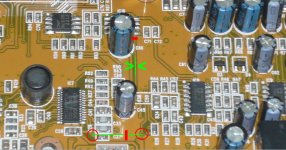
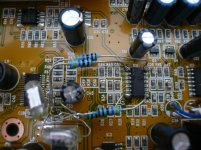
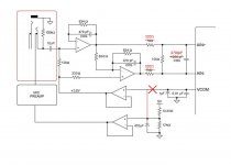
I attached another photo that hopefully is more clear. You have to cut the trace close to the op amp (Vcom buffer) at the point marked with red color. To the bottom of the photo, near the audio codec, I have marked another trace that is on the bottom layer of the pcb. It connects the trace coming from the Vcom buffer to audio codec's pin #15 (Vcom out). I cut that too in an attempt to minimize any interference related to the high frequency peak. You may leave it and see how it does when cut only close to the op amp.I have a few questions.
Where exactly do I cut the pcb traces in the photo below.(I cant see the cuts)
Also, why is pin 5 -pin 3 bridged? It is not shown on the AN241 schematic. (It bridges one opamp input + to second opamp input + ?)
View attachment 778928
The "Vcom buffer" is a dual op amp. Both halves are doing DC buffer duties meaning they take DC from a high impedance source and deliver the same DC at a very low impedance. The half that involves pin #5 input is taking the DC source from the audio codec's pin #15 and send it to bias the ADC input buffer (AD8694) as shown on the AN241. I found that this scheme was responsible for the high frequency peak. So I needed another DC source to feed the op amp's pin #5. The other half of this op amp that involves pin #3 is taking DC from a voltage divider fortunately at the same level as Vcom. So, cutting the trace close to pin #5 and bridging it to pin #3 results to feeding both #3 and #5 from the same voltage divider.
Yes, the white wire is the ground. I tried it both connected and disconnected and although it didn't make any difference I preferred to leave it floating because the input is grounded when connected to the output anyway in a loop measurement. You may try for yourself. I'm thinking to install a switch to allow floating or grounded mode.Also your TRS input shows an ground which I am guessing is the white wire on the top right? Why is it disconnected?
View attachment 778929
Last question is are the electrolytic caps removed the same as on the input TRS schematic diagram?
Yes, I used the same caps. Please watch the polarity. I have connect them reversed wrt their original orientation. See the schematic.
Attachments
Last edited:
Warning!
Today the soundcard all of a sudden stopped working... It was the input buffer op amp, the AD8694. It just fried and sorted Vcc to ground. I removed it and the soundcard recovered, except input signal of course. The audio codec is fine. I've been jeopardizing this thing for almost two months now but I was very careful, hard to believe I broke something. And the Vcom tweak also applies to the output/headphones stage which seems OK. So, the op amp output resistors mod is where I focus at the moment. Maybe Behringer engineers had reasons to put highish value output resistors there -and the shunt resistors also. Maybe there is a major oscillation problem causing the high frequency peak and eventually fried the op amp? I'll replace it and see what it does. Meanwhile please be careful with this mod. The op amp didn't fry immediately, it worked fine during all these days and I never checked temperatures. Please do that or better wait for news. Apologies for any inconvenience.
Today the soundcard all of a sudden stopped working... It was the input buffer op amp, the AD8694. It just fried and sorted Vcc to ground. I removed it and the soundcard recovered, except input signal of course. The audio codec is fine. I've been jeopardizing this thing for almost two months now but I was very careful, hard to believe I broke something. And the Vcom tweak also applies to the output/headphones stage which seems OK. So, the op amp output resistors mod is where I focus at the moment. Maybe Behringer engineers had reasons to put highish value output resistors there -and the shunt resistors also. Maybe there is a major oscillation problem causing the high frequency peak and eventually fried the op amp? I'll replace it and see what it does. Meanwhile please be careful with this mod. The op amp didn't fry immediately, it worked fine during all these days and I never checked temperatures. Please do that or better wait for news. Apologies for any inconvenience.
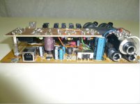
While I'm waiting for parts to come from overseas, I did some reading and experimentation. The audio codec chips of this kind -not cirrus logic in particular- seem to have some requirements in circuit implementation that won't allow deviations. They demand DC coupling with the input buffer at half the rail voltage be it from Vcom output or a simple voltage divider. That was made clear from my findings so far. Another thing is that they want the input buffer to be connected to the same power supply. So, if a +/- 15V op amp is going to be used as an input buffer, then the audio codec should be fed from this psu via regulators. This is hard to implement on the UMC 202. What I tried was an off board buffer designed on the cirrus logic application notes schematic with NE5532 and an isolated DC booster.(see pics) With volume controls down it has a very nice noise floor, but when start to increase signal it seems to run out of headroom very early.
So, a 5V op amp seems a sensible choice and at a first glance the AD8694 is perfect for the job. Cmos, high slew rate, high current, low impedance, rail to rail output. Alas... The audio codec chips need to have the so called "antialiasing capacitor" right on their input. To make things worse, cirrus logic chips require a much bigger cap -2,7n- compared to other chips that ask for pF. Capacitive load is what op amps hate most in general, but Cmos parts are even more sencitive to this. That's why behringer used so big output resistors shunted with another one paralleled to the antialiasing cap. But that means signal attenuation and the most the souncard could do with that scheme was -17dB. The mod presented in post #17 was an attempt to fix this, but the result was a fried AD8694 because of oscillation. So, please do not proceed with this mod. The other two steps seem fine and since I've got so close to an acceptable performance, I'll try a few more things. I want to see at what point the resistors could be lowered without causing problems and even build an off board buffer based on AD8694.
So, a 5V op amp seems a sensible choice and at a first glance the AD8694 is perfect for the job. Cmos, high slew rate, high current, low impedance, rail to rail output. Alas... The audio codec chips need to have the so called "antialiasing capacitor" right on their input. To make things worse, cirrus logic chips require a much bigger cap -2,7n- compared to other chips that ask for pF. Capacitive load is what op amps hate most in general, but Cmos parts are even more sencitive to this. That's why behringer used so big output resistors shunted with another one paralleled to the antialiasing cap. But that means signal attenuation and the most the souncard could do with that scheme was -17dB. The mod presented in post #17 was an attempt to fix this, but the result was a fried AD8694 because of oscillation. So, please do not proceed with this mod. The other two steps seem fine and since I've got so close to an acceptable performance, I'll try a few more things. I want to see at what point the resistors could be lowered without causing problems and even build an off board buffer based on AD8694.
Attachments
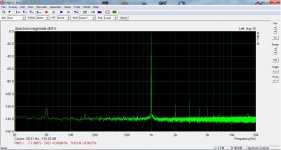
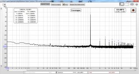
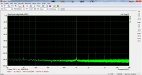
I've entered peak season in my job, but i found some time to work on this. I've acquired a smd rework station and replaced the bad op amp. Also, I restored the factory status i.e. removed all modifications and started looking at it step by step with a little better understanding now. Surprise again..! The high pitched noise is now gone by its own, no Vcom buffer mod applied!!! First attached is the current status and the second is what it supposed to be the same when I started this project, reattached from post#1. I'm clueless about this. I don't know what caused this as all functions seem OK and same to the original. I mean, I am satisfied by the result but completely unable to explain how it could be duplicated. I just keep it. However, the Vcom buffer mod also proved efficient.
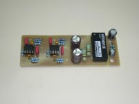
So, what's left is to increase the dB level. At full throttle as explained in previous posts, besides it was catastrophic, made it up to -8dB at best. The third attached is how it does now -stock status. THD+N is the same with the modified, but for THD I managed down to 0,00025% before. I'll try to take it again as close to that but the experiments won't be on the soundcard. I made a small "evaluation board" with the AD8694 so I can play. I googled for some insight on this subject and came across this Op Amps Driving Capacitive Loads | Analog Devices. It gives a different explanation about the op amp configuration with respect to Cirrus Logic. Instead of an antialiasing filter they suggest phase margin restoration against the capacitive load. I've read it a couple of times but I'll need many more and still not sure how deep I could get. Anyway, I believe to reach to a result by next weekend.
PS. Meanwhile, I've been playing... An application notes "copy and paste" without deviations. With through hole parts. That was the easy part. It needs a USB to i2s converter. The plan is to reverse engineer Behringer's pcb and transplant the chips hopefully with their conscious intact i.e. make use of the proprietary drivers. Winter's project.
So, what's left is to increase the dB level. At full throttle as explained in previous posts, besides it was catastrophic, made it up to -8dB at best. The third attached is how it does now -stock status. THD+N is the same with the modified, but for THD I managed down to 0,00025% before. I'll try to take it again as close to that but the experiments won't be on the soundcard. I made a small "evaluation board" with the AD8694 so I can play. I googled for some insight on this subject and came across this Op Amps Driving Capacitive Loads | Analog Devices. It gives a different explanation about the op amp configuration with respect to Cirrus Logic. Instead of an antialiasing filter they suggest phase margin restoration against the capacitive load. I've read it a couple of times but I'll need many more and still not sure how deep I could get. Anyway, I believe to reach to a result by next weekend.
PS. Meanwhile, I've been playing... An application notes "copy and paste" without deviations. With through hole parts.
That was the easy part. It needs a USB to i2s converter. The plan is to reverse engineer Behringer's pcb and transplant the chips hopefully with their conscious intact i.e. make use of the proprietary drivers. Winter's project.Attachments
The paper linked above is very informative. And provides practical examples from where I got an idea. It is the "out-of-loop compensation" case, what Behringer's engineers have used. It stabilizes the op amp against the capacitive load but it steals signal and the suggested workaround is to increase the gain of the op amp. Seems quite straightforward but I could use some help here.
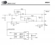
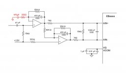
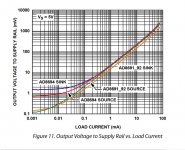
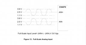
The first pic shows the signal level requirements to drive the ADC input. The driver is an AD8694 op amp, rail to rail output, working at 5V (+/-2,5V) and set to unity gain. Currently, it swings +/-1,4V. Theoretically, it could swing +/-2,5V or close to that. From datasheet short circuit current is +/-80mA. The second pic shows output voltage Vs load current. With this info, here is what I'm thinking to do:
The third pic is what the soundcard holds on board. It is a SE to BAL converter set to unity gain and floating at 2,5V (Vcom). The idea is to add the red parts i.e. to increase the gain. Only the non inverting stage needs that, the inverting will just make an antiphase copy. I wouldn't like to change anything else as all seem critical for stability. But this means a "heavy" feedback loop. My interpretation is that with G=2 and the output current ability of the op amp there should not be any problem. Do I miss anything here? I wouldn't like to find out the hard way once again... Also, would this affect poles and zeros? It is mandatory to maintain the phase margin of the circuit.
Attachments
Adding some gain to this stage is basically sound, since your input common-mode range only reaches to +3.9 V on this particular opamp, so +/-1.4 V is the limit now indeed. You don't need quite this much though - 806 ohms (+100 µF) would do just fine, for a gain of 1.78 (5 dB). Going from having to drive 634 ohms to 440 ohms seems a bit less daunting than the same with 382 ohms.
More good news: As you add gain, your stability margins only go up.
Do experiment with lowering the 1 kOhm resistor value again. 91 ohms might have been too low, so try 220-470 ohms perhaps.
Now with extra gain in front of the ADC, the question is, where are we going to take away gain to make up for it?
Another question is, how are we going to get a decent input stage again, now that the regular one is bypassed? An unbalanced input is all fine and dandy but will only go so far. Have you had a look at the input circuitry at all? Is it similar to the Rod Elliott balanced mic pre, or is it something else altogether? I mean, if in doubt you could just use an external portable mixer as a mic preamp / balanced receiver, but still.
Nice! Thanks for response! I'll try things and see how it goes. The preamp section is a stack of op amps together with some discrete parts, a design under the name "Midas", aiming to musicality rather than hifi. I'm not interested in this section but I haven't disabled it completely. I used a switched jack so I can have bypassed or functional front panel inputs. Just in case I learn to play the guitar...
However, I realize the benefits of differential inputs. I keep the attached schematic in the back of my mind.
However, I realize the benefits of differential inputs. I keep the attached schematic in the back of my mind.
Attachments
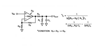
Some progress has been made. I tried the idea to increase the gain tweaking the feedback network. It does increase gain but as a consequence, distortion increased too. I wasn't even able to get the performance I had without it. So, back to theory... The schematic is taken from the paper mentioned above. The formula gives the "zero" introduced by the output resistor Rx and the load capacitor CL. "To ensure stability, the value of Rx should be such that the added zero (fz) is at least a decade below the closed loop bandwidth of the op amp circuit". AD8694 datasheet states Gain Bandwidth Product =10MHz and Full Power Bandwidth =360kHz. 10MHz seems too much to explain what is happening here so I take the 360kHz. According to the formula, the soundcard as comes from the factory with Rx=1kohm, RL=10kohm and CL=1nF has a fz~ 170kHz. My mod with the 91 ohm resistors pushed fz at 1,6MHz! No wonder the results... However there is a way to decrease this resistor by increasing CL. Indeed the 1nF is small compared to the 2,7nF suggested by the audio codec datasheet. Theoretically, we can keep fz at 170kHz with CL=2,7nF and Rx=1k//470=320ohm. That's what I did and it's already close to the target keeping RL (10kohm) in place. This resistor doesn't seem to affect fz considerably so the plan is to remove it once again. Perhaps later in the evening.
Attachments
Some more thoughts on this. Previous post didn't take in account the RC feedback network. This should introduce another pole and zero isn't it? And at quite high frequency. Does this add to the fz as calculated above? That would mean that simply by removing those little caps from the feedback it would enable the returning of the 91Ω resistors... Or am I completely out of track?
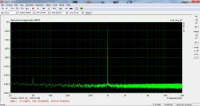
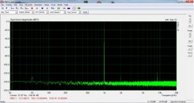
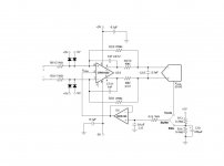
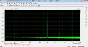
During the last week I've been testing the sound card with and without the 10k load resistor -RL in post #54. Although it makes a difference in signal level, I always had to bring it down to -8dB (with ARTA as a reference) for best performance. So, eventually I left this resistor on for reliability. The best this soundcard -or me- can do is shown in first and second pics. Third pic is a schematic with all the modifications. Mic preamps bypass as explained in post #16 with corrected schematic at post #23. Vcom buffer mod as explained in posts #18 and #46.
The op amp output resistors final mod:
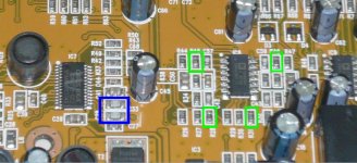
The fourth pic shows the resistors in the green frame that have to be reduced from 1k to 320Ω and the capacitors that have to be increased from 1nF to 2,7nF. Last pic is how I did it. P2P 470Ω in parallel with the existing 1k and 1,5nF in parallel with the 1nF. Quick and dirty way to test but it works fine so it stayed.
The op amp output resistors final mod:
The fourth pic shows the resistors in the green frame that have to be reduced from 1k to 320Ω and the capacitors that have to be increased from 1nF to 2,7nF. Last pic is how I did it. P2P 470Ω in parallel with the existing 1k and 1,5nF in parallel with the 1nF. Quick and dirty way to test but it works fine so it stayed.
Attachments
Just attempted this mod and the improvement is huge! very similar to your measurements. This is awesome, all umc owners who intended to do measurements should see this.


Before mod, front panel input at -1.7dbfs

The hf spike disappeared when I just finished and cut the top trace, but it comes back few days later. I tried cutting the bottom trace too but didn't change a thing. Tho now it is 20db lower then before cutting the top trace so its fine.

Also is there a reason why you chose 320ohm? I tried lowering it to 200 and the thd+n dropped from 0.0023% to 0.0017. Is there a point where the opamp starts to oscillate? And is it a must to increasing the cap value? For me, changing it to 2.7nf sightly increased the distortion.
Thanks
Before mod, front panel input at -1.7dbfs
The hf spike disappeared when I just finished and cut the top trace, but it comes back few days later. I tried cutting the bottom trace too but didn't change a thing. Tho now it is 20db lower then before cutting the top trace so its fine.
Also is there a reason why you chose 320ohm? I tried lowering it to 200 and the thd+n dropped from 0.0023% to 0.0017. Is there a point where the opamp starts to oscillate? And is it a must to increasing the cap value? For me, changing it to 2.7nf sightly increased the distortion.
Thanks
... ...Also is there a reason why you chose 320ohm? I tried lowering it to 200 and the thd+n dropped from 0.0023% to 0.0017. Is there a point where the opamp starts to oscillate? And is it a must to increasing the cap value? For me, changing it to 2.7nf sightly increased the distortion.
Thanks
Everything is explained in posts #48, #49 and #50. I found out the hard way... The paper linked in post #50 allows to calculate the safety margin. Generally, the lower the output resistor becomes, the bigger the antialiasing cap has to be. OTOH, distortion will increase with big resistor and/or cap. 320 ohm is the 1k ohm originally on board bypassed with 470 ohm just for convenience. And I increaced the cap to 2,7n because that's what Cirrous Logic datasheet suggests. I would advice not to push too much. Those opamps are really sensitive.
About the high frequency spike: it never appears in the same position and the Vcom buffer mod gives me the feeling that it works like an antiphase cancellation somewhere
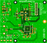
 rather than a cure in the first place. I think it's something about the clocks. I've been working on this soundcard the whole winter -see attachment, nothing presentable yet. The pcb layout is a nightmare, interference is quaranteed...
Attachments
- Home
- Design & Build
- Equipment & Tools
- Behringer UMC 202HD for measurements