According to the data here: Analog-to-digital converter - Wikipedia the 25 ps jitter of the NB3N511, in the path of the external clock, should lead to a very noticeable degradation of the performance for frequencies beyond 10kHz.
Could you check this please once the ADC is functional?
Could you check this please once the ADC is functional?
According to the data here: Analog-to-digital converter - Wikipedia the 25 ps jitter of the NB3N511, in the path of the external clock, should lead to a very noticeable degradation of the performance for frequencies beyond 10kHz.
Could you check this please once the ADC is functional?
May be overkill, but something like Si5345 could do it with much lower jitter.
According to the data here: Analog-to-digital converter - Wikipedia the 25 ps jitter of the NB3N511, in the path of the external clock, should lead to a very noticeable degradation of the performance for frequencies beyond 10kHz.
Could you check this please once the ADC is functional?
Hello zfe,
I know the NB3N511 isn't jitter killer, but keep in mind that it come from
an isolated interface that can itself introduce much jitter.
The external clock is not mandatory, there is already an on board low very low jitter clock.
You can note too (as already say in my post #9) that the external clock can be used
for re-synchronization of the ADC sampling to external DAC system.
And yes of course I will do measurements tests with internal/external clock
input when all will be ready
") .
.Frex
Hello,
Some news today about the project (I admit much less interesting than the first black holes pict !).
I received the small panel PCB for the Leds and encoder from JLCpcb.
They seem to have done good job.
So , I finished to solder all others parts and wired the new panel PCB.
And now, it's time to test this !
I work on a test CPLD first to check all I/O and then started in the real
CPLD design. Much work coming.
Below few pics of what it look like for now.
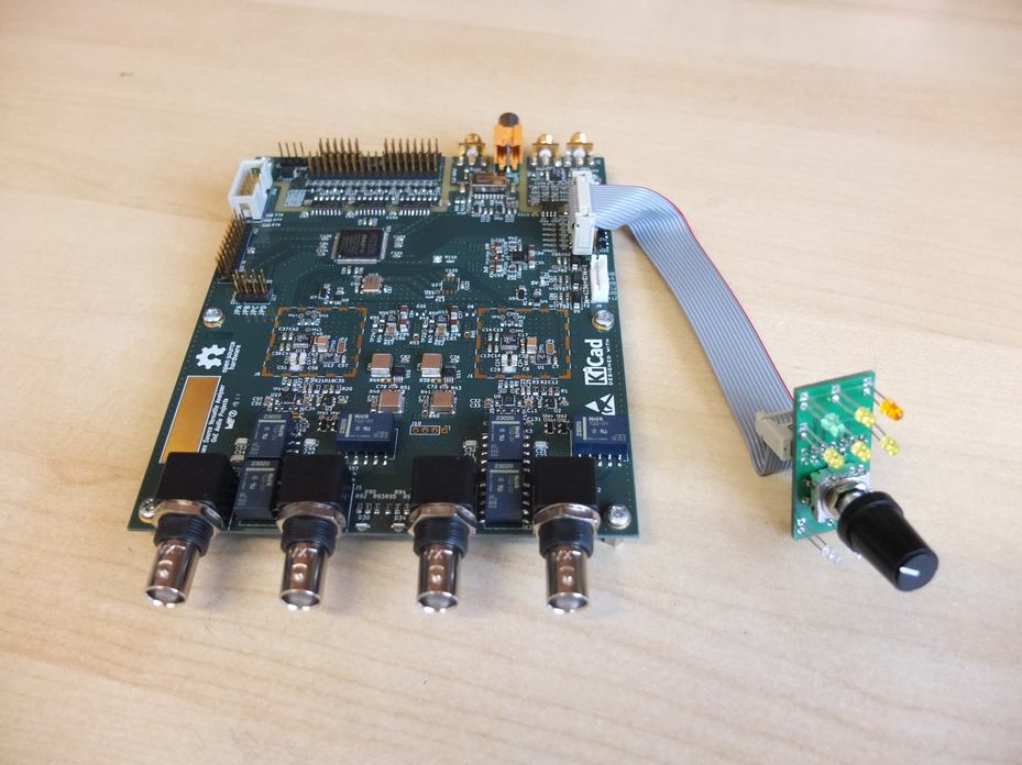
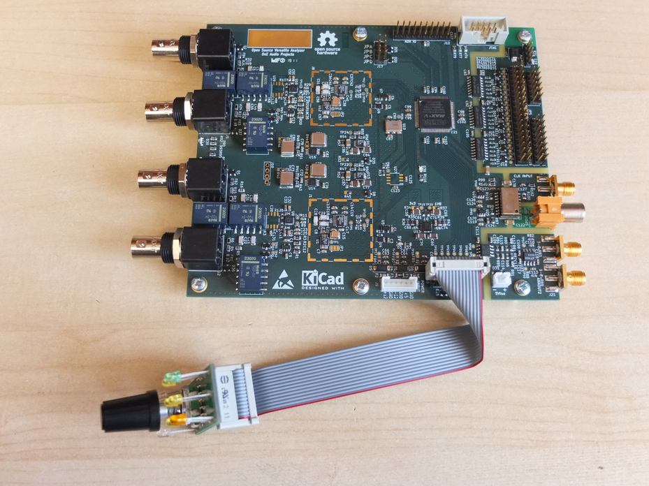
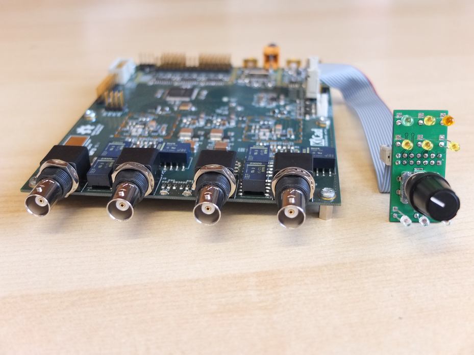
Frex
Some news today about the project (I admit much less interesting than the first black holes pict !).
I received the small panel PCB for the Leds and encoder from JLCpcb.
They seem to have done good job.
So , I finished to solder all others parts and wired the new panel PCB.
And now, it's time to test this !
I work on a test CPLD first to check all I/O and then started in the real
CPLD design. Much work coming.
Below few pics of what it look like for now.
Frex
Hi HpW,
Might you have a link to this? I did a search on the internet and on minidsp's website and nothing came up ...
Cheers,
Jesper
May on interest,
minidsp announced a 8x384khz multichannel streamer, but not slave clock capability O
Hp
Might you have a link to this? I did a search on the internet and on minidsp's website and nothing came up ...
Cheers,
Jesper
Hi HpW,
Might you have a link to this? I did a search on the internet and on minidsp's website and nothing came up ...
Cheers,
Jesper
MCHStreamer - USB Audio Swiss-Army knife
May on interest,
minidsp announced a 8x384khz multichannel streamer, but not slave clock capability O
Hp
I have my doubts, as this would need a higher data rate than supported by the USB2 Audio standard.
It supports 8 channels "and" 384kHz, but also 8 channels AT 384kHz?
In the User manual I e.g. for I2S a limitation to 10 channels at 192kHz.
@HpW & zfe:
Thanks to HpW for the feedback. Reading a bit into the product brief for this MCH streamer I notice this specification:
To me this would mean up to eight channels in AND out at 24/32 bits ... unless their way of stating performance is a bit "camouflaged".
Hmmm ... I think I will leave it here but thanks again HpW for the info.
Cheers,
Jesper
Thanks to HpW for the feedback. Reading a bit into the product brief for this MCH streamer I notice this specification:
I2S: Up to 8ch bidirectional audio - 24/32bit up to 384kHz
To me this would mean up to eight channels in AND out at 24/32 bits ... unless their way of stating performance is a bit "camouflaged".
Hmmm ... I think I will leave it here but thanks again HpW for the info.
Cheers,
Jesper
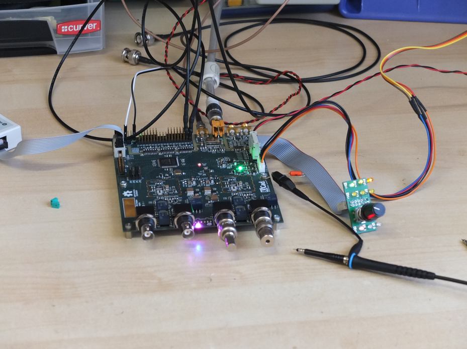
AA2380v1 first test
Hi all,
I finished the first test CPLD, and programmed the AA2380 board successfully.
The test software allow to test all I/O to check board connections.
It test also the front panel encoder/leds board.
These first checks give :
-- SE/DIFF & filters Relays drive ==> OK
-- external encoders and leds ==> OK
-- isolated high speed external clock circuit ==> OK
-- Two isolated oscillator sync analog outputs ==> OK
-- S/PDIF isolated output ==> OK
-- 192kHz LTC2380-24 ADC SPI reading and send to S/PDIF ==> OK
-- Front tri-color status LEDs drive ==> OK
-- All high-speed Isolated I/O loop-back ==> OK
-- Un-isolated Test connector I/O control ==> OK
-- Config jumper test ==> OK.
-- external PLL clock test ==> Not done (NB3N511 not yet installed).
The ADC data sent to S/PDIF show very flat and artifact free spectrum,
that's looks very promising...
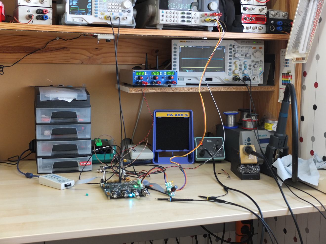
Little pictures of the test in progress on my bench these days :
Now, I must now work on the final CPLD software to use averaging process
and allow SR speed control, and many others things.
I already started to write a document in order to specify what i expect exactly
for each block. Much job again to do, but that progress continuously...
I work also in a parallel way on the AAPSU01 design (power supply board) ,
i will post soon more info about it.
Frex
Hi all,
I finished the first test CPLD, and programmed the AA2380 board successfully.
The test software allow to test all I/O to check board connections.
It test also the front panel encoder/leds board.
These first checks give :
-- SE/DIFF & filters Relays drive ==> OK
-- external encoders and leds ==> OK
-- isolated high speed external clock circuit ==> OK
-- Two isolated oscillator sync analog outputs ==> OK
-- S/PDIF isolated output ==> OK
-- 192kHz LTC2380-24 ADC SPI reading and send to S/PDIF ==> OK
-- Front tri-color status LEDs drive ==> OK
-- All high-speed Isolated I/O loop-back ==> OK
-- Un-isolated Test connector I/O control ==> OK
-- Config jumper test ==> OK.
-- external PLL clock test ==> Not done (NB3N511 not yet installed).
The ADC data sent to S/PDIF show very flat and artifact free spectrum,
that's looks very promising...
Little pictures of the test in progress on my bench these days :
Now, I must now work on the final CPLD software to use averaging process
and allow SR speed control, and many others things.
I already started to write a document in order to specify what i expect exactly
for each block. Much job again to do, but that progress continuously...
I work also in a parallel way on the AAPSU01 design (power supply board) ,
i will post soon more info about it.
Frex
Hey Frex,
Wonderful! If you’re going to sell bare boards please put me down for one.
Me too! Amazing open source attitude!
AAPSU01 - OSVA Power supplt board design
Hello all,
Thanks for comments.
DIYralf, sorry i don't have recorded my first FFT measurement.
I must make some software job inside CPLD before to make serious measurements.
Anyway, i started another part of the analyzer, the AAPSU01 power circuit board.
I recall it's specifications :
Because it can be very interesting to use the AAPSU01 power supply board in others
application than the OSVA, and so it is possible to customize many things :
-Each Low noise LDO can be omitted for no noise critical applications. (bypass resistors).
-Symmetric Outputs voltages can be configured to any values between about +/-6V to +/- 15 V.
You can see the full AAPSU01 synoptic below :
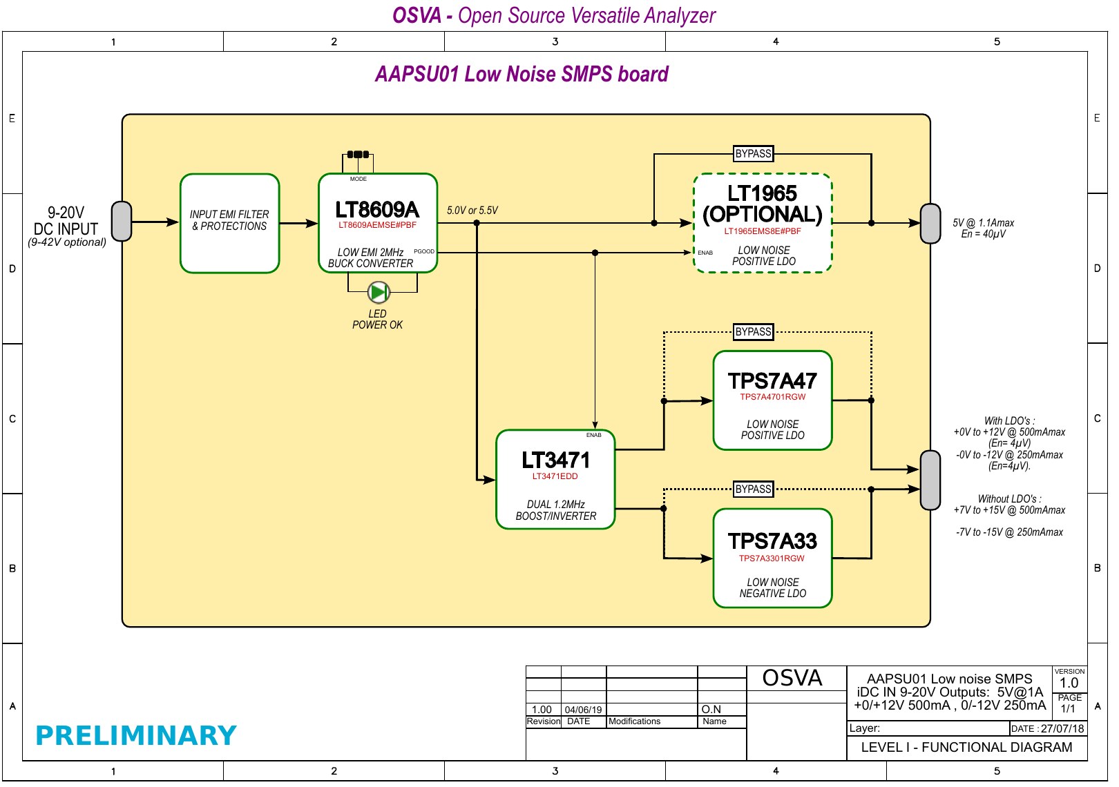
You can download it in pdf form here : AAPSU01_synoptic-V0.pdf
The full Kicad schematics of the design can be show below :
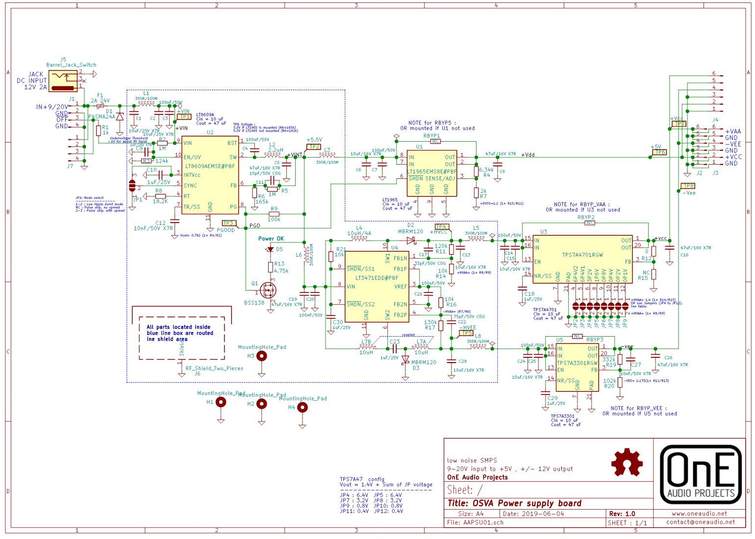
You can download it in pdf form here : AAPSU01_sch.pdf
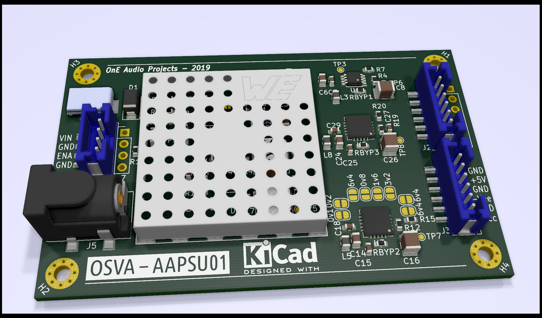
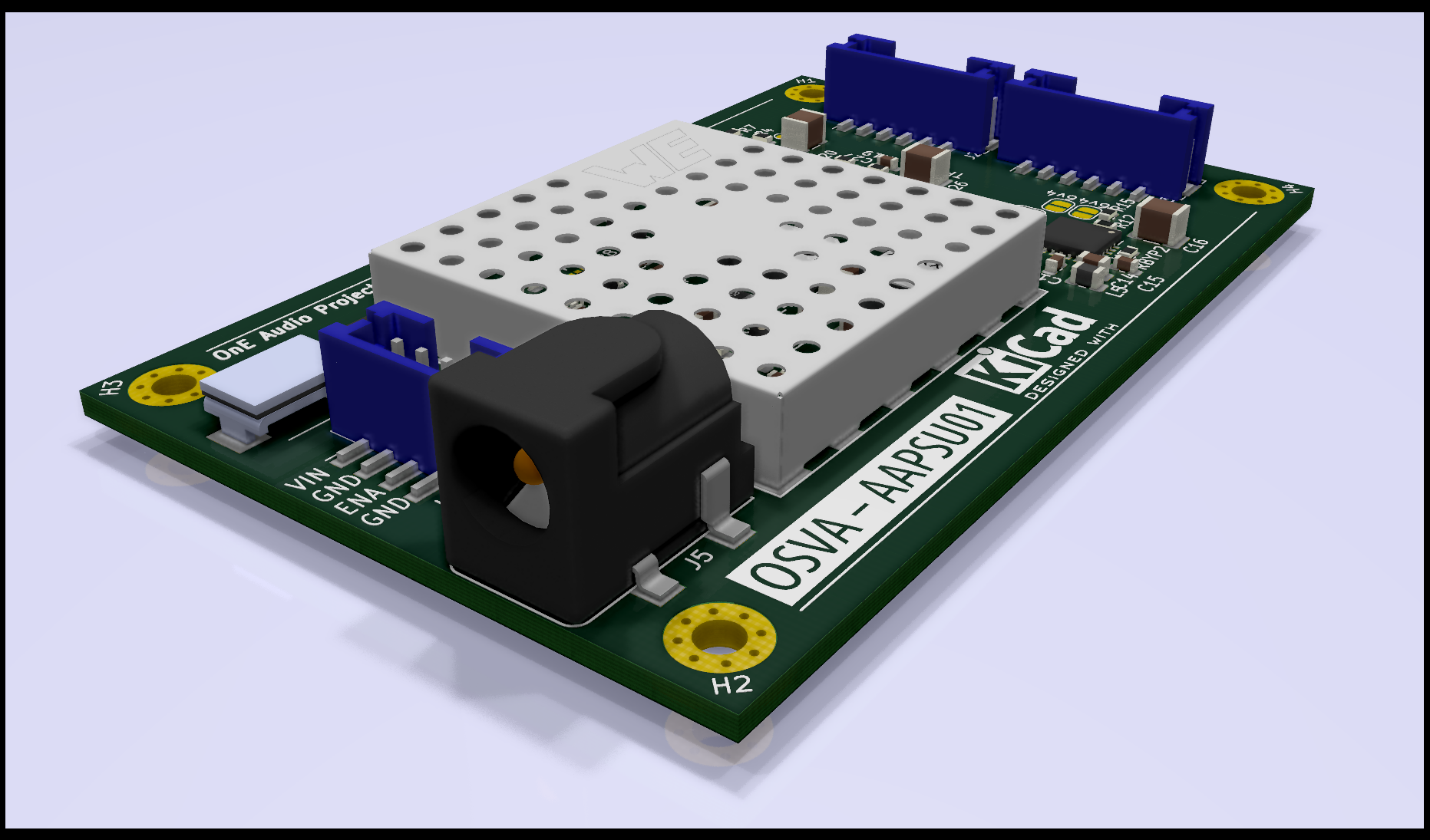
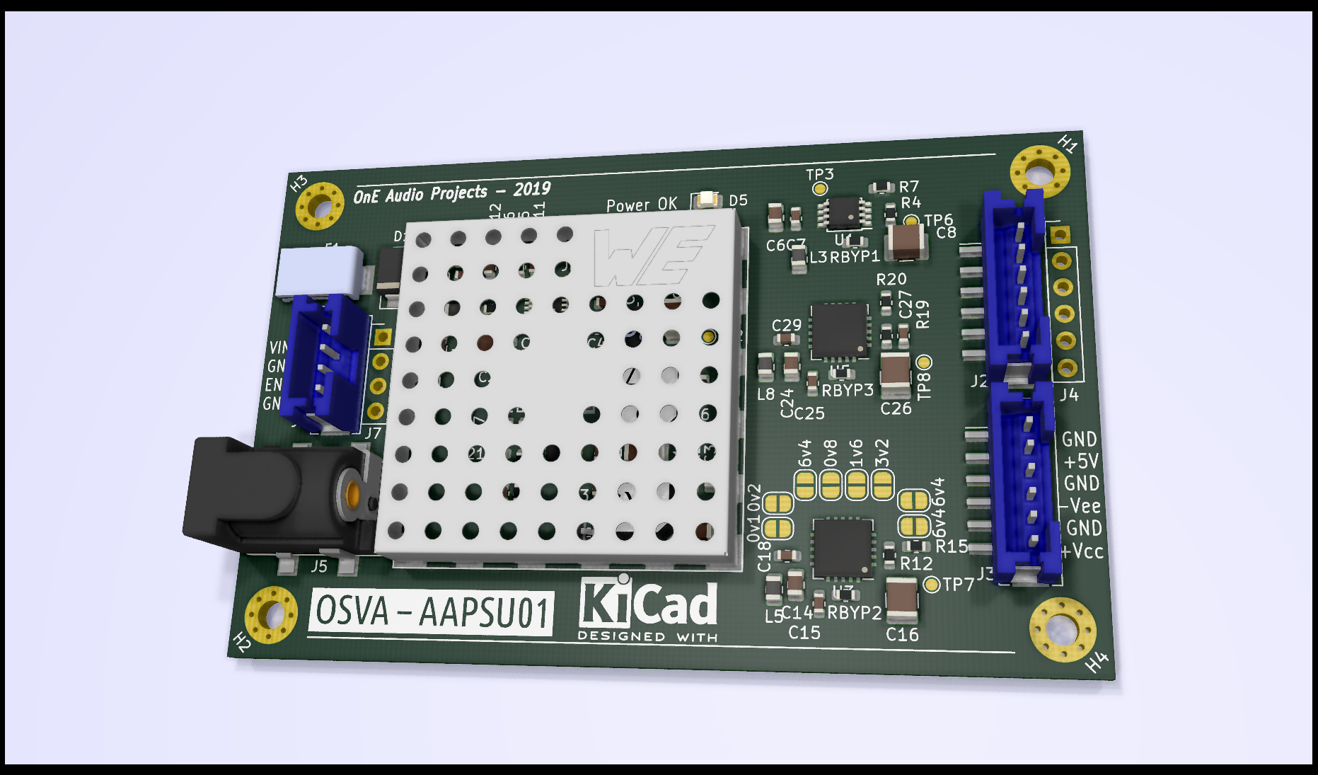
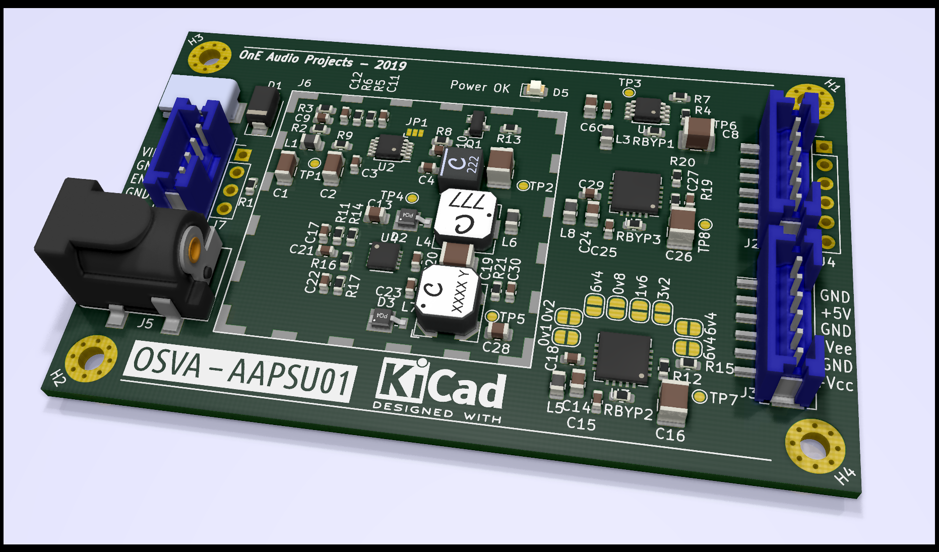
I imported and placed all parts before to route, and so you can show how it would looks like soon in my hands on the pictures below (Kicad 3D rendering view).
I now must start to route tracks , and so let's go.
To follow... ;o)
Comments welcomed !
Frex
Hello all,
Thanks for comments.
DIYralf, sorry i don't have recorded my first FFT measurement.
I must make some software job inside CPLD before to make serious measurements.
Anyway, i started another part of the analyzer, the AAPSU01 power circuit board.
I recall it's specifications :
- Nominal input voltage 12Vdc (9-20V range, extendable to 42V).
(coming from Lithium batteries or wall adapter) - 3 x ultra low noise regulated outputs :
]5 VDC @ 1A max (En= 40µVrms / 10Hz-100kHz )
+12 VDC @ 500mA max (En= 4µVrms / 10Hz-100kHz )
-12 VDC @ 500mA max (En= 4µVrms / 10Hz-100kHz ) - High overall efficiency by using switch mode converter and low noise post regulator.
- Over-voltage and over-current protection.
- Low EMI emission (use LinearTech low EMI Silent Switcher IC).
- Optional shield for switching regulators.
- 4 Layers PCB design.
- Power ok led indicator.
- TTL enable input.
- Ultra low quiescent current.
- Small PCB size (50 x 80mm).
- Input/output connectors are JST-PH 2mm or standard 2.54mm pin header.
- 4 x 2.5mm mounting holes.
Because it can be very interesting to use the AAPSU01 power supply board in others
application than the OSVA, and so it is possible to customize many things :
-Each Low noise LDO can be omitted for no noise critical applications. (bypass resistors).
-Symmetric Outputs voltages can be configured to any values between about +/-6V to +/- 15 V.
You can see the full AAPSU01 synoptic below :
You can download it in pdf form here : AAPSU01_synoptic-V0.pdf
The full Kicad schematics of the design can be show below :
You can download it in pdf form here : AAPSU01_sch.pdf
I imported and placed all parts before to route, and so you can show how it would looks like soon in my hands on the pictures below (Kicad 3D rendering view).
I now must start to route tracks , and so let's go.
To follow... ;o)
Comments welcomed !
Frex
Hi,
Yes of course.
The switching regulator allow itself to minimize influence from a poor (noisy) source,
and the output low noise LDO's regulators has themselves a very high PSSR for high ripple and noise rejection.
Of course all of this would be confirmed by real measurements of output noise in various conditions.
Frex

Hello astromo,
Thank you.
The project is progressing step by step, and not so fast than i would like. Anyway, i very motivated and i try to go ahead.
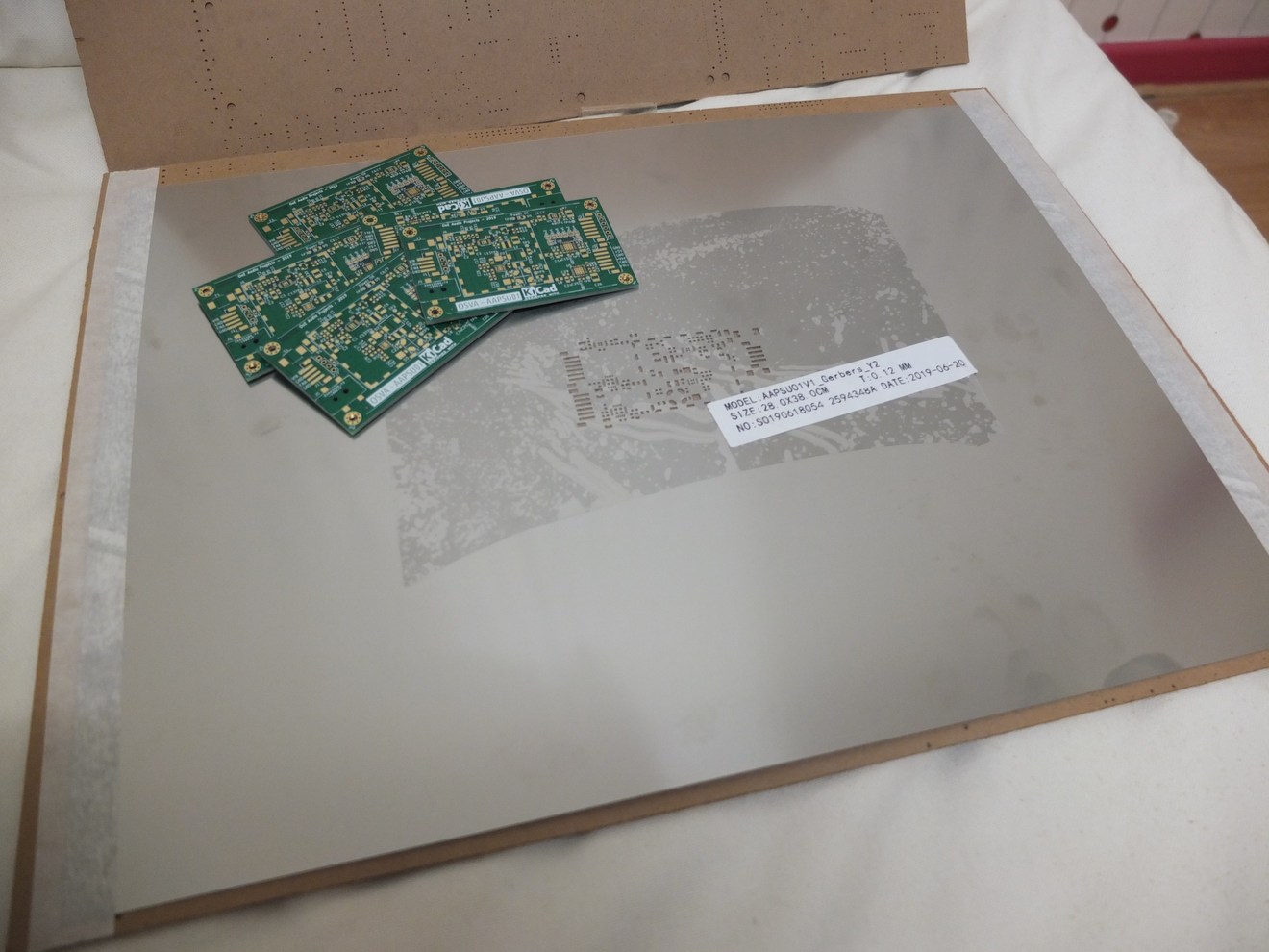
I received today the third PCB of the OSVA project, the AAPSU01 board. This is the first PCB i ordered wit it's stencil.
I will go to holidays soon, so there will be a slight pause.
But i will come back in great fettle to keep going !
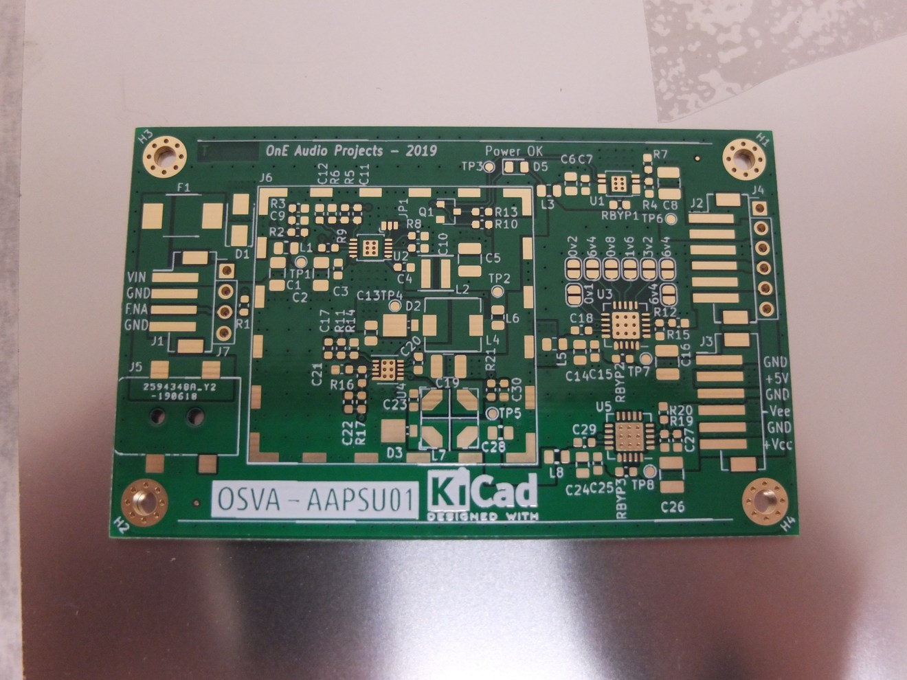
Frex.
Thank you.
The project is progressing step by step, and not so fast than i would like. Anyway, i very motivated and i try to go ahead.
I received today the third PCB of the OSVA project, the AAPSU01 board. This is the first PCB i ordered wit it's stencil.
I will go to holidays soon, so there will be a slight pause.
But i will come back in great fettle to keep going !
Frex.
- Home
- Design & Build
- Equipment & Tools
- OSVA - Open source Versatile Analyzer