Hi there,
Some time ago, I built myself a measurement preamp, and I also made a tentative 10x transformer to extend the measurement range:
https://www.diyaudio.com/forums/equ...000-measurement-preamplifier-post5663580.html
Everything works satisfactorily, but the improvised transformer is somewhat limited for the low frequencies: it reaches a few tens of hertz, and it can even be pushed to 10Hz, if the source impedance is ~zero, but that is neither ideal or comfortable.
The obvious solution is to use something bigger, but it also increases the bulk, and the sensitivity to external stray fields.
This is why I experimented with other solutions.
The first tested is an old favorite: it uses a synchronous modulator (=chopper)/demodulator combined with a high frequency transformer.
Thanks to the modulation, the size of the transformer can be made arbitrarily small, and the frequency range extends to DC.
The main challenges reside in the modulator: the switches need to have a really low Rdson (no greater than 200mΩ, and preferably much lower to allow for other parts of the circuit), be perfectly ohmic, and generate no crap of their own, like charge-injection spikes.
Such a marvel is pure fantasy, of course, which is why I adopted a pragmatic, low-tech approach:
Closest to ideal are ordinary, switching MOSfets: they are almost ideal regarding Rdson, ease of control, ohmicity and bilaterality (not true at high levels, but at the µV level, it holds perfectly true).
They are also cheap and widely available.
The only "small" problem is the charge-injection aspect: the typical G-D capacitance is in 10's or even 100's of pF, and at a nV level sensitivity, it cannot be ignored, when the control signal reaches 10V p-t-p.
Charge-injection is going to be a prevalent problem, even with high performance switches and sophisticated compensations, which is why I didn't spend a lot of effort there.
Instead, I concentrated on the post-processing aspect, which has the most potential for gains.
As the circuit is exploratory and experimental, I included the possibility of many variations: the clock frequency can be varied in a 1 to 20 ratio, the transformer is overdesigned, etc
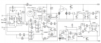
After a number of iterations and tentatives, I ended up with this circuit:
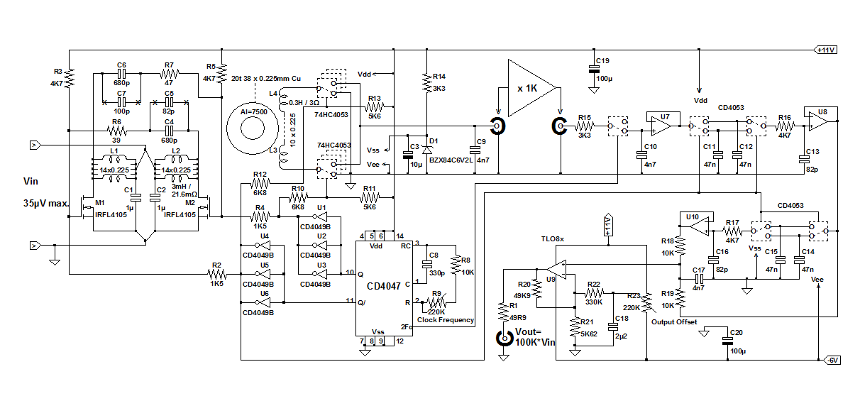
It is far from perfect, but it works and would even be usable if properly cased, connectorized and supplied.
The components are completely ordinary and non-critical: mylar and X7R caps, commodity ICs, and the transformer is built from home-made twisted wire and a bog-standard, suppression-grade ferrite core.
My initial goal was to cover the 0 to 100Hz frequency range, because that is where the need is greatest, but I tried to reach 1kHz, as a best effort.
In the end, the -3dB bandwidth is 2.5kHz, with a clock frequency of 8kHz.
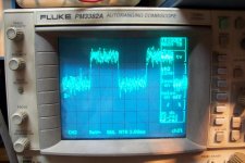
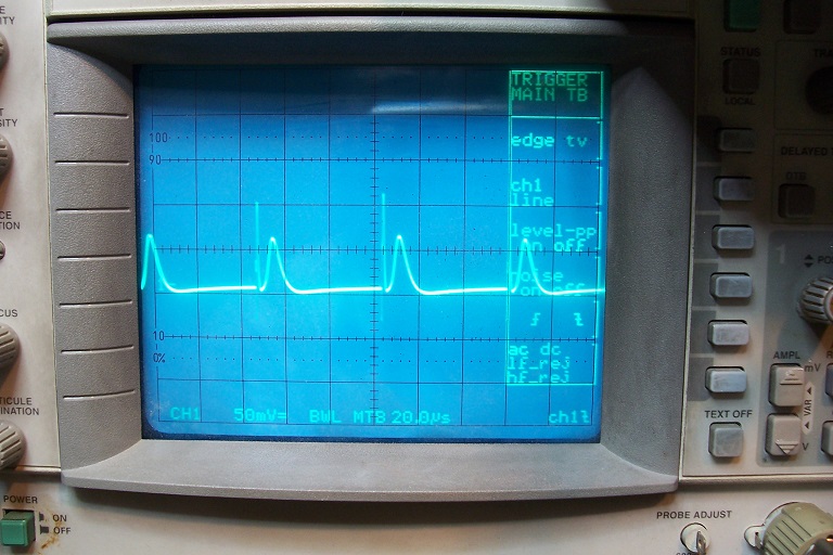
Here is the output with a 100Hz, 100nV pp squarewave input.
The oscillogram is the real-time, raw output: no averaging or processing of any kind.
The waveform is noisy, obviously, but perfectly identifiable:

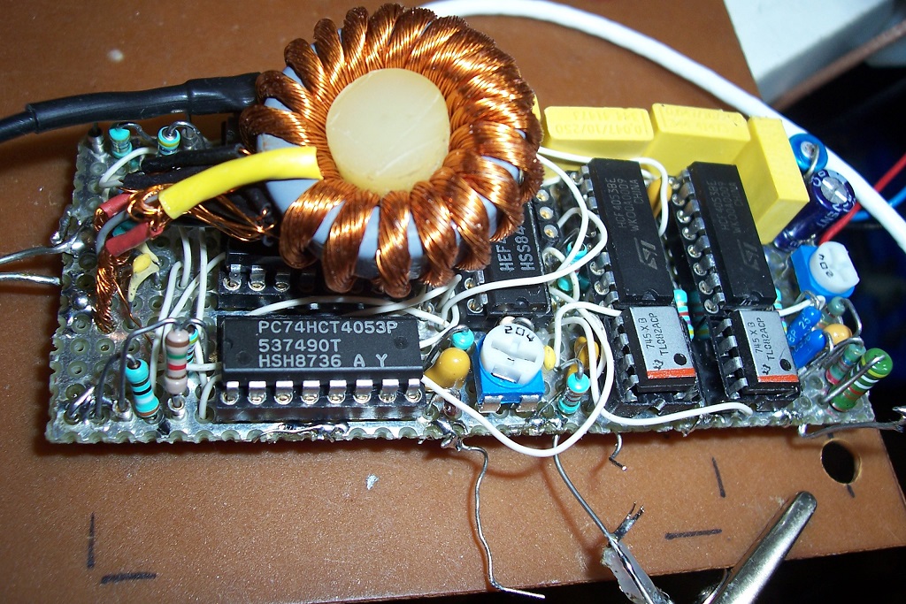
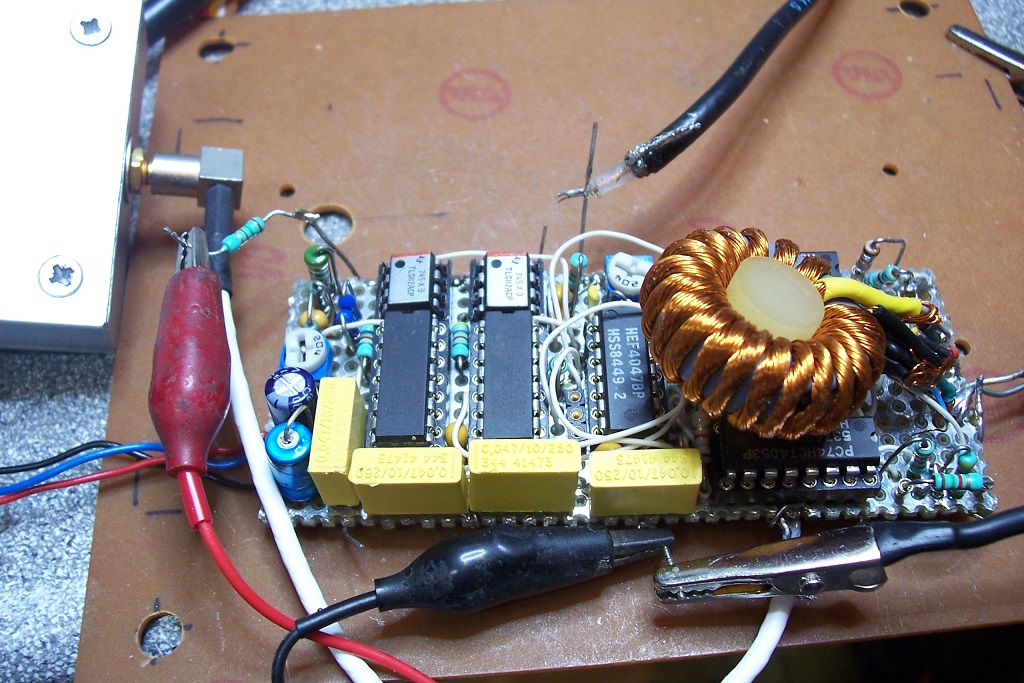
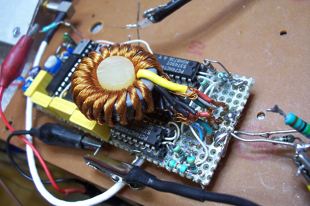
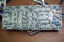
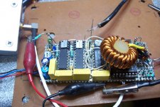
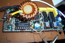
Here are some pics of the prototype:

Some time ago, I built myself a measurement preamp, and I also made a tentative 10x transformer to extend the measurement range:
https://www.diyaudio.com/forums/equ...000-measurement-preamplifier-post5663580.html
Everything works satisfactorily, but the improvised transformer is somewhat limited for the low frequencies: it reaches a few tens of hertz, and it can even be pushed to 10Hz, if the source impedance is ~zero, but that is neither ideal or comfortable.
The obvious solution is to use something bigger, but it also increases the bulk, and the sensitivity to external stray fields.
This is why I experimented with other solutions.
The first tested is an old favorite: it uses a synchronous modulator (=chopper)/demodulator combined with a high frequency transformer.
Thanks to the modulation, the size of the transformer can be made arbitrarily small, and the frequency range extends to DC.
The main challenges reside in the modulator: the switches need to have a really low Rdson (no greater than 200mΩ, and preferably much lower to allow for other parts of the circuit), be perfectly ohmic, and generate no crap of their own, like charge-injection spikes.
Such a marvel is pure fantasy, of course, which is why I adopted a pragmatic, low-tech approach:
Closest to ideal are ordinary, switching MOSfets: they are almost ideal regarding Rdson, ease of control, ohmicity and bilaterality (not true at high levels, but at the µV level, it holds perfectly true).
They are also cheap and widely available.
The only "small" problem is the charge-injection aspect: the typical G-D capacitance is in 10's or even 100's of pF, and at a nV level sensitivity, it cannot be ignored, when the control signal reaches 10V p-t-p.
Charge-injection is going to be a prevalent problem, even with high performance switches and sophisticated compensations, which is why I didn't spend a lot of effort there.
Instead, I concentrated on the post-processing aspect, which has the most potential for gains.
As the circuit is exploratory and experimental, I included the possibility of many variations: the clock frequency can be varied in a 1 to 20 ratio, the transformer is overdesigned, etc
After a number of iterations and tentatives, I ended up with this circuit:
It is far from perfect, but it works and would even be usable if properly cased, connectorized and supplied.
The components are completely ordinary and non-critical: mylar and X7R caps, commodity ICs, and the transformer is built from home-made twisted wire and a bog-standard, suppression-grade ferrite core.
My initial goal was to cover the 0 to 100Hz frequency range, because that is where the need is greatest, but I tried to reach 1kHz, as a best effort.
In the end, the -3dB bandwidth is 2.5kHz, with a clock frequency of 8kHz.
Here is the output with a 100Hz, 100nV pp squarewave input.
The oscillogram is the real-time, raw output: no averaging or processing of any kind.
The waveform is noisy, obviously, but perfectly identifiable:
Here are some pics of the prototype:
Attachments


The noise performance is not ideal, which comes as no surprise, but it is encouraging: I measured the total noise level in a 10Hz to 1kHz bandwidth (that is the most convenient for me at the present time; I will try to come up with more focused figures later).
The 1kHz upper limit is defined by a simple RC network.
In those conditions, the total noise of the LNA alone, with its input shorted, is a shade under 30nV.
When the LNA is placed in the virtual transformer context, still with its input shorted, this becomes 35nV: this may look surprising, but just connecting the grounds is sufficient to raise the level, despite my extreme precautions.
At this sensitivity level, all interconnections and possible ground loops become a major headache, which is why I try to build all my gear as class II devices, but even so, the 10's of µA of inter-ground leakage currents are sufficient to cause troubles.
The GND of the VT is certainly also a little "hot" from a RFI perspective, because of the digital circuits.
When the short is moved to the VT input, the input referred noise becomes 5nV (=50nV for the LNA input), which means a degradation of ~3dB.
That's 3dB too much, of course, but for an experimental circuit such as this one, it is definitely encouraging, keeping in mind that the only shielding is a summary electrostatic one (a piece of PCB material slipped under the circuit), with no magnetic shielding at all. That's to be compared with the double mu-metal shield required by the traditional copper and iron transformer.
When the input short is replaced by a 1Ω resistor, the noise becomes 7.5nV, meaning the equivalent noise resistance is a bit under 1Ω.
There is certainly room for improvement(s): when I average the waveform with a mains sync, I can see that a significant proportion of the noise increase is caused by mains-related artifacts (the LNA itself is almost perfectly clean).
In fact, when I used a crocodile clip to make a steady short during the measurements (a clip alone, with the jaws making the short; using a wire would be disastrous), I realized that there was a small but significant increase in mains-related noise, compared with the provisional short made with a piece of copper wire held by hand.
It took me some time to understand that the steel of the alligator clip concentrated the ambient magnetic stray fields towards the tiny loop area of the short, causing the increase in hum level.
Amazing performance. Gerhard has been working on something similar to measure without 1/F noise. My version of the G = 1000 low noise measurement amp (for Ikoflexer).
Being very lazy (and busy) I'll wait until someone makes some PCB's for this. But its really promising. Any sense on DC performance (offset, drift etc.)?
Being very lazy (and busy) I'll wait until someone makes some PCB's for this. But its really promising. Any sense on DC performance (offset, drift etc.)?
I didn't pay a lot of attention to this aspect: the amplification chain includes the LNA as the first gain block after the demod, and it is AC coupled.Any sense on DC performance (offset, drift etc.)?
I just made a check: with the input shorted, the DC offset is <1µV (input referred), but I cannot be more accurate without making a proper measurement setup and thermally insulating the input section, because thermocouple effects are going to dominate.
When the input is left completely open, this becomes ~60µV, and doesn't look particularly stable.
I think that it is caused mostly by residual charge-injection artifacts that are synchronously rectified by the MOSfets and appear as a DC voltage across the input capacitors: I didn't care very much about charge-injection compensation, because it is tackled later in the processing chain.
Here is a general description:
The beating heart of the circuit is its master clock oscillator, based on a CD4047.
Why the 4047?
It is easily available, cheap, and does the job perfectly well, since the clock doesn't need to be particularly stable or jitter-free.
In addition, it has low skew, complementary outputs and also a 2*Fo output which comes handy in this circuit.
As I didn't know what frequency I was going to adopt, I made it variable from 3 to 60kHz.
The main outputs are buffered by 3 CD4049 each, more to be able to face all possible situations than to meet a specific need.
The outputs drive the modulator MOSfets through 1.5K resistors.
Their role is two-fold: they slow the signal edges thanks to the gate capacitance, and combined with the two 4.7K resistors, they shift the level so that the low level is just under the threshold voltage.
This reduces charge-injection considerably, because most of it takes places when the MOS is OFF.
As soon as it is ON, the drain is shorted to the source (=GND), and injection is practically completely shunted.
It would be possible to do even better with temperature-compensated, individually adjustable voltages, but I didn't feel the need to go that far.
Cross-connected capacitors C4 to C7 compensate charge injection to the first order, with R6 R7 as a final refinement.
These compensations remain relatively crude, and are far from sufficient to recover a half-clean signal at the output of the demodulator.
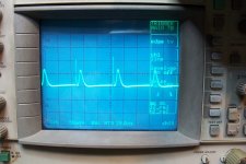
Here is the output of the LNA (with a x10 probe):
The useful signal is much smaller, and is completely drown in the clock-related artifacts (it is invisible here).
This means that the LNA must have particularly good properties of linearity, dynamic range and slew-rate to be able to preserve the tiny signal against much larger amplitude crud.
The modulator uses a half-bridge (push-pull) rather than a full one, because it means only one Rdson in the path, and much less charge-injection effects: two of the MOS would be floating between the input and output arms.
The transformer is of a peculiar construction: it has a single 20 turns winding, but it is multi-strand: 38 exactly.
Two times 14 are used for the primaries and are parallel-connected, and the remaining 10 are series-connected to form the secondary.
This arrangement results in exceptional performances: the total secondary-referred leakage inductance is only 10µH, to be compared with the 300mH magnetizing inductance.
This transformer is overdesigned, to be able to cope with various clock frequencies and various configurations: in particular, the number of turns of 20 is not a coincidence, it is a multiple of 10.
This means that, in theory, I could use a 2 x 2 turns primary to reach a "voltage gain" of 100.
In principle, it should be possible: milliohm level MOSfets are widely available. Would it find an actual use?
I doubt it, but who knows...
The beating heart of the circuit is its master clock oscillator, based on a CD4047.
Why the 4047?
It is easily available, cheap, and does the job perfectly well, since the clock doesn't need to be particularly stable or jitter-free.
In addition, it has low skew, complementary outputs and also a 2*Fo output which comes handy in this circuit.
As I didn't know what frequency I was going to adopt, I made it variable from 3 to 60kHz.
The main outputs are buffered by 3 CD4049 each, more to be able to face all possible situations than to meet a specific need.
The outputs drive the modulator MOSfets through 1.5K resistors.
Their role is two-fold: they slow the signal edges thanks to the gate capacitance, and combined with the two 4.7K resistors, they shift the level so that the low level is just under the threshold voltage.
This reduces charge-injection considerably, because most of it takes places when the MOS is OFF.
As soon as it is ON, the drain is shorted to the source (=GND), and injection is practically completely shunted.
It would be possible to do even better with temperature-compensated, individually adjustable voltages, but I didn't feel the need to go that far.
Cross-connected capacitors C4 to C7 compensate charge injection to the first order, with R6 R7 as a final refinement.
These compensations remain relatively crude, and are far from sufficient to recover a half-clean signal at the output of the demodulator.
Here is the output of the LNA (with a x10 probe):
The useful signal is much smaller, and is completely drown in the clock-related artifacts (it is invisible here).
This means that the LNA must have particularly good properties of linearity, dynamic range and slew-rate to be able to preserve the tiny signal against much larger amplitude crud.
The modulator uses a half-bridge (push-pull) rather than a full one, because it means only one Rdson in the path, and much less charge-injection effects: two of the MOS would be floating between the input and output arms.
The transformer is of a peculiar construction: it has a single 20 turns winding, but it is multi-strand: 38 exactly.
Two times 14 are used for the primaries and are parallel-connected, and the remaining 10 are series-connected to form the secondary.
This arrangement results in exceptional performances: the total secondary-referred leakage inductance is only 10µH, to be compared with the 300mH magnetizing inductance.
This transformer is overdesigned, to be able to cope with various clock frequencies and various configurations: in particular, the number of turns of 20 is not a coincidence, it is a multiple of 10.
This means that, in theory, I could use a 2 x 2 turns primary to reach a "voltage gain" of 100.
In principle, it should be possible: milliohm level MOSfets are widely available. Would it find an actual use?
I doubt it, but who knows...
Attachments
The demodulator is based on the ubiquitous 74HC(T)4053: it doesn't have high performances, but it is cheap and easy to source, and here the three channels are paralleled, resulting in a switch resistance of less than 15Ω, which is fit for the purpose.
The supply arrangement is a bit unusual: the total voltage is 11V, to lower the channel resistance, but this means that Vss has to float 5V below Vdd.
The 0V is also the signal ground, which would normally not be acceptable under normal circumstances, but since the maximum signal excursion will never exceed 1mV in positive or negative, it is a perfectly acceptable expedient here.
This also means that resistive translators are required for the control inputs.
As the demodulator is a full-bridge, it could, in principle, be used to cancel the noise of the secondary's resistance. That is not the "core business" of the synchronous mod-demod, but it could in principle do it (within the limits allowed by the theory, of course).
It is probably not a good idea though, and I didn't attempt to use it (the winding resistance is 3Ω): here, the ratio of the clock frequency to the max signal frequency is low, and anyway, it would generate more out of band noise to filter.
The input windings are outside the protection of the synch. process: the two windings are separate, meaning the LF noise generated by their resistance is uncorrelated.
The transformer-based transfer means that galvanic isolation of the input and output is implicit, but I didn't make use of it, something I bitterly regret.
I reasoned that for an experimental circuit, the (minor) complication of isolating the digital control signals was not worth the trouble, but I was completely wrong: at this sensitivity level, interconnections and ground loops become such a headache that any relief is welcome.
It must be noted that the mod/demod section has no protection against aliasing, except C1 and C2 which attenuate the HF components of the input signal in a rather informal way.
Ideally, a true LPF should be used, but given the level of impedance and the sensitivity, it wouldn't be easy, and if the source impedance is really low and unwanted HF components are expected, the simplest solution is probably to increase the value of the input cap.
A cursory look would suggest you could use a FET bridge and optodrivers or a transformer to drive the FET bridge. Since this is essentially a form of sampling you could use a sample and hold to capture the desired value at the optimum time at the output of the second bridge and ignore the transients. I hope I am understanding this correctly.
Davida showed a neat trick using an ADC plus a DAC as a sample and hold.
Davida showed a neat trick using an ADC plus a DAC as a sample and hold.
Do you mean as the input modulator, or later in the processing?A cursory look would suggest you could use a FET bridge and optodrivers or a transformer to drive the FET bridge.
The current half-bridge configuration works satisfactorily, and the total resulting resistance is ~70 mΩ, much lower than it is required
Later in the processing, there is a filter-and-hold and an alternate resampler.Since this is essentially a form of sampling you could use a sample and hold to capture the desired value at the optimum time at the output of the second bridge and ignore the transients. I hope I am understanding this correctly.
The demodulator is a kind of sample-hold too, with C9 as Hold capacitor.
At this level, I have attempted to introduce a small dead time, of a few µs, to discard the instants just following the switchings, which contains most of the transients.
However, the cure made the problem worse, because of charge injection effects.
This is before the LNA, and the level is extremely low: well under 1mV.
The strategy I used was to amplify the whole, and make the process at a level 1,000x higher.
The first part is the filter-and-hold, gated by the 2*F clock signal: it leaves out the first half of the cycle, and conducts for the latter part, when "the dust has settled".
This is followed by the alternate resampler: each capacitor C10 C11 is alternatively written and read, and the output always sees a clean, steady signal, taken in exactly identical cycle after cycle.
This completely eliminates clock-related artifacts, provided the two half cycle (and thus the input circuits) are perfectly symetrical, which is achievable.
In principle, this should be sufficient, and I managed to have it working perfectly, but in the end I decided to add another resampler, because of weird effects.
First, the balancing is possible but finnicky, and if it is imperfect, the result is a leakage of the clock frequency in the output: one resampler is sufficient to eliminate all even multiple of the clock, but not the odd order ones, including the fundamental itself.
When the transformer is exposed to external magnetic fields, it has a flux-gate like behavior, and also leaks the fundamental.
I couldn't find a satisfactory explanation, but the effect is present and quite annoying.
For these reasons, I added a second resampler, and the outputs are continuously and accurately averaged by R18 R19, thus eliminating completely the fundamental and other odd order components.
The result is spotlessly clean, very robust, and does not require accurate adjustments.
Note that I was open-minded about the filtering strategy: I also considered a passive filter, combined or not with a resampler.
I managed to make all the variants work, but the inductor of the passive filter was problematic because of its size and sensitivity to LF fields.
It would have required a serious mu-metal shield.
In the end, the performance of the resampler(s) proved sufficient, and they brought much less problems and complications
I have continued the exploration of some unexpected aspects of this "transformer".
One of them is the input resistance: I stumbled on a anomalously low input resistance, between 15Ω and 25Ω depending on circumstances.
This resistance is difficult to predict accurately, but this is way below any reasonable expectation.
In the end, I tracked down the anomaly to a cross-conduction of the modulating push-pull:
The low level is shifted just below the MOSFETs threshold (to minimize charge injection), but combined with the edge control, it results in an increase in the conduction times, meaning they overlap, causing a dramatic reduction in input resistance.
In principle, a non-overlapping control should solve the problem, but this does not seem to be completely the case.
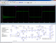
This example is an overlapping-corrected drive: the red and blue traces are the gate signals, and the yellow trace is the reference for the threshold, and there is no overlap.

Yet, when we look at the voltages across R7 feeding the modulator, a resistance of ~40Ω can be inferred.(Magenta trace= output of V3, green trace after R7)

This means that high-amplitude transients on the gate seem to affect the very-small signal conductivity of the FET.
It remains to be seen whether the sim and reality behaviors are absolutely identical, but they certainly show convergence.
One of them is the input resistance: I stumbled on a anomalously low input resistance, between 15Ω and 25Ω depending on circumstances.
This resistance is difficult to predict accurately, but this is way below any reasonable expectation.
In the end, I tracked down the anomaly to a cross-conduction of the modulating push-pull:
The low level is shifted just below the MOSFETs threshold (to minimize charge injection), but combined with the edge control, it results in an increase in the conduction times, meaning they overlap, causing a dramatic reduction in input resistance.
In principle, a non-overlapping control should solve the problem, but this does not seem to be completely the case.
This example is an overlapping-corrected drive: the red and blue traces are the gate signals, and the yellow trace is the reference for the threshold, and there is no overlap.
Yet, when we look at the voltages across R7 feeding the modulator, a resistance of ~40Ω can be inferred.(Magenta trace= output of V3, green trace after R7)
This means that high-amplitude transients on the gate seem to affect the very-small signal conductivity of the FET.
It remains to be seen whether the sim and reality behaviors are absolutely identical, but they certainly show convergence.
Attachments
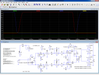
I have now modified my prototype to eliminate the crossconduction completely.
The strategy I opted for was to send the switching waveforms practically directly to the gates of the MOSfets, without transition control, and to rely entirely on a shifted-level gate signal to eliminate most of the injection effects.
R5 allows an accurate adjustment of the low-level state at 3V, the threshold voltage of the IRFL4105.
Small compensation capacitors are still present, and I have also reactivated the blanking generator R4/R26/C5: now it does a useful job.
As a result, the input resistance has increased, but only to 60Ω, meaning some of the weird effects seen in sim have some base in reality.
Anyway, 60Ω is not large, but it is sufficient considering the application.
The modification has only affected the resistance: all other parameters, noise performance in particular are strictly unchanged.
Attachments
- Status
- This old topic is closed. If you want to reopen this topic, contact a moderator using the "Report Post" button.
- Home
- Design & Build
- Equipment & Tools
- A bit of fun exploring this noise-oriented, virtual transformer