I am going to build myself a half-decent LNA, and logically I am going to base it on The Master's design:
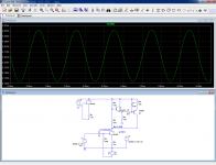
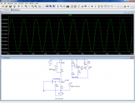
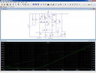
My version of the G = 1000 low noise measurement amp (for Ikoflexer).
I will customize it though, mainly because I want to use a particular FET.
I have heaps of older types, and I spotted the J110 (process NIP), which is capable of reaching the 1nV/√Hz level @1kHz, but technology of the previous generation imposes difficult constraints, unlike the 2SK170 or BF869: parameters like Idss, Vth, transconductance are inextricably correlated, making the task of extracting a sufficient gain at a sufficient current and without exceeding the dissipation very difficult.
I had considered using a high voltage (~100V) supply combined with a drain resistance of several K, but I would prefer a more elegant and less power-hungry solution.
Here is the idea I came up with: if I can make a 25mA CCS having a sufficiently low noise compared to the FET, I could use a standard 15V supply and still benefit of an amplification ~=µ.
To meet the condition, I came to the conclusion that R4 needs to be significantly larger than the 1/s of the FET (supposing that the FET and the BJT have a similar noise voltage, which will normally not be the case, especially for a PNP).
Before actually starting to build anything, I would like to be sure that my conclusion is valid, and that I have not overlooked some obscure effect like partition noise or else that could poop the party.
This kind of circuit needs to be built with care and attention, and it would be unpleasant to discover at the end that the thing is useless because of an unforeseen problem
Attachments
By the way, on this occasion I also noticed a bizarre quirk of LTspice XVII:
The configuration of a voltage source inside a CCS drives it completely berserk, without good reason: amplitudes are low but normal, and the timestep of 1µ should be small enough.
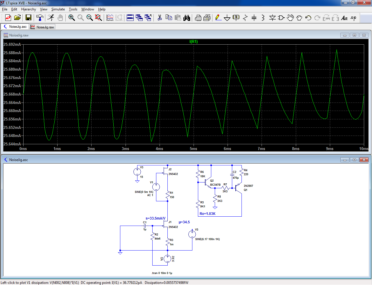
To get something normal, the timestep has to be reduced to 20ns, which is ridiculous for a sim processing 1kHz.
There must be seriously wrong truncating strategies or something of the kind.
Since ADI took over LT, things seem to go downhill....
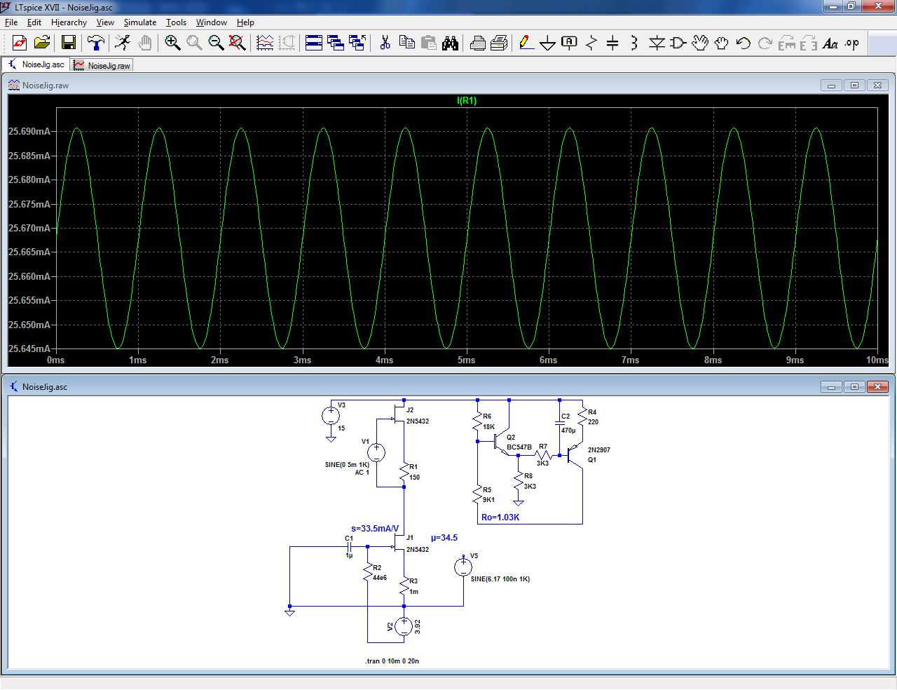
The configuration of a voltage source inside a CCS drives it completely berserk, without good reason: amplitudes are low but normal, and the timestep of 1µ should be small enough.
To get something normal, the timestep has to be reduced to 20ns, which is ridiculous for a sim processing 1kHz.
There must be seriously wrong truncating strategies or something of the kind.
Since ADI took over LT, things seem to go downhill....
Attachments
Getting convergence around fet circuits has been a challenge for me with LTspice for years. I just bumble through until it makes sense.
I have used J110's for low noise inputs for years. Sorting helps. I cascode them with enhancement mode mosfets and try to keep the Vds pretty low to keep the self heating down. I run them at around 5 mA. There is not a lot to gain running them higher. Paralleling is also possible. Cascoding is important if input C is important since with gain the Miller cap makes the input C pretty high. Cascoding reduces that a lot.
You don't need a lot of gain at the first stage, just enough that the En input of the first stage is 6 or more dB more than the second stage contribution. LTspice has a great tool for that.
Thanks for the interesting and valuable advice.
The cascode crossed my mind, but it looked too easy, too simple, and I didn't dig deeper, thinking there had to be some kind of snag...
May I ask why your preference goes to a MOSFET (and not a BJT) for the cascode?
Regarding the current, there is a little to be gained for a largish increase: the difference between 0.1*Idss and 0.01*Idss is worth some trouble (Idss can be ~500mA!):
Attachments
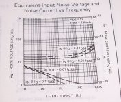
Below is the original specs for the J108-J110 from National (who originated it). I was confused by the spec showing 500 mA Idss. In any case cranking the drain current doesn't make a big difference and will bring a major thermal penalty. In "Low-noise electronic design, by C. D. Motchenbacher and F. C. Fitchen" they go into the details on why that's counterproductive.
The best way to explore would be to build a tester (or get access to a Quan-Tech) and see what you can learn.
I use the power mosfets because they are simple to use (no complex biasing) they don't add noise and you can use up to 200V if you really need to.
If this is for measurement you could simplify it with an opamp for most of the gain. See the schematic and LTspice file attached. I did not use a J110 model (not sure I have one). Its oversimplified but both the biasing and the drain current can be done very simply. Its also a simplified version of the Quan-Tech transistor input circuit.
Paralleling does work but matching is a pita, especially after the first set. And you may need a lot to meet your target noise level.
I cheated and built a low noise preamp using a transformer for the input. Its probably the best way to get ultra low noise if you can work with the limitations of a transformer. I think the one I built has an equivalent input noise of about 5 Ohms (.3 nV/rtHz). I used a geoformer for the input from eBay. They are rare but do pop up. Limited in HF but extend down pretty far without major 1/f penalties.
Attachments
In fact, the 500mA Idss does not apply to the J110: in the Siliconix databook, the detailed datasheets are for processes, not individual type numbers.Below is the original specs for the J108-J110 from National (who originated it). I was confused by the spec showing 500 mA Idss.
The J110 is one of the lowest Idss selection of the NIP process.
I have also found BF246's in my stock, and on paper at least, they look more promising than the J110.
I agree that excesses in one direction or the other are counterproductiveIn any case cranking the drain current doesn't make a big difference and will bring a major thermal penalty. In "Low-noise electronic design, by C. D. Motchenbacher and F. C. Fitchen" they go into the details on why that's counterproductive.
I think that I will not be able to escape the construction of a "draft"The best way to explore would be to build a tester (or get access to a Quan-Tech) and see what you can learn.
I will use the 1,000x Scott's circuit, but even with the cascode, the gain will be marginally too low if I use reasonable opamps (~10nV/√Hz) with a standard 12 or 15V supply.If this is for measurement you could simplify it with an opamp for most of the gain. See the schematic and LTspice file attached. I did not use a J110 model (not sure I have one). Its oversimplified but both the biasing and the drain current can be done very simply. Its also a simplified version of the Quan-Tech transistor input circuit.
If I use both the cascode and the low-noise CCS, I will have enough gain for a modest noise penalty, and I will be able to work with standard +/-15V supplies and have a low capacitance as a bonus.
I hesitated: most of my needs will be low or very impedance, so I could have opted for bipolars and have a lower noise easily, but of course there will always be the exception where I will need a higher impedance, and if I build something, I prefer to keep it relatively general.I cheated and built a low noise preamp using a transformer for the input. Its probably the best way to get ultra low noise if you can work with the limitations of a transformer. I think the one I built has an equivalent input noise of about 5 Ohms (.3 nV/rtHz). I used a geoformer for the input from eBay. They are rare but do pop up. Limited in HF but extend down pretty far without major 1/f penalties.
With the FET LNA, I will probably be able to find or to modify a transformer in case I need an extra low noise level at a very low impedance
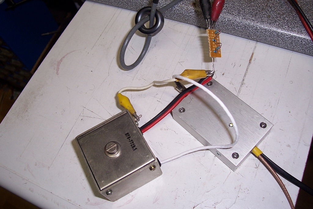
Update: I have now built the "draft" (a very crude one).
It is just the FET under test, a cascode and some bias and bypass circuits.
The drain load is a 1K8 WW resistor (to minimize excess noise), and the adjustment is completely manual: it is a PITA given the gain and the large time constants, but it is manageable for a limited number of tests.
The drain supply is 50V, as I make the tests @ Id=25mA
I also included the possibility of interchanging the cascode transistor, including the MOS/BJT option. Not that I thought it was going to change anything, but since it is almost free at the design stage, I included it.
As expected, the type or breed of transistor didn't matter at all , but it is always nice to have hard evidence, even for the obvious.
With this setup, a run-of-the-mill J110 gave 0.27µV total noise in a 10kHz BW (figures are indicative, at this stage I am not looking for absolute accuracy).
The BF246 which should have been marginally better was in fact marginally worse.
I also tested a variety of other samples: 2SK125, 2N4860, ... without too many illusions, and unsurprisingly they were slightly worse than the BF246.
Interesting things were yet to come: I tested a NS J110, and it came out at 0.2µV, already better than Siliconix, but the real winner was from Teledyne-Philbrick, with 0.17µV.
Certainly better than what I expected, and the setup + environment is far from ideal: the construction is shielded, obviously, but it is open, and many equipments converge to the GND: oscilloscope, two supplies, microvoltmeter, generator, multimeter.
I have PLC in my house, a mobile relay antenna is located less than 100 meter away and the lighting of my lab is half traditional fluorescents, half LED.
With a proper build, completely enclosed in a diecast case and with ground paths under control I can certainly expect some improvement.
I will also make proper arrangements to keep the FET as cool as possible, which is not the case now (dissipation is 25mA x 6V, 150mW)
To summarize, the experiment was really worth the trouble
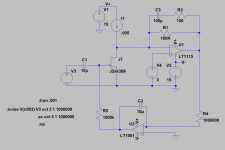
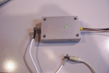
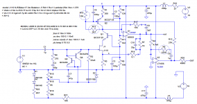
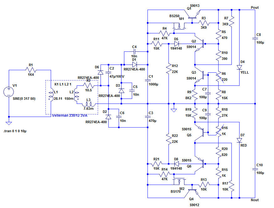
I have now finalized the design and construction of my x1000 probe:
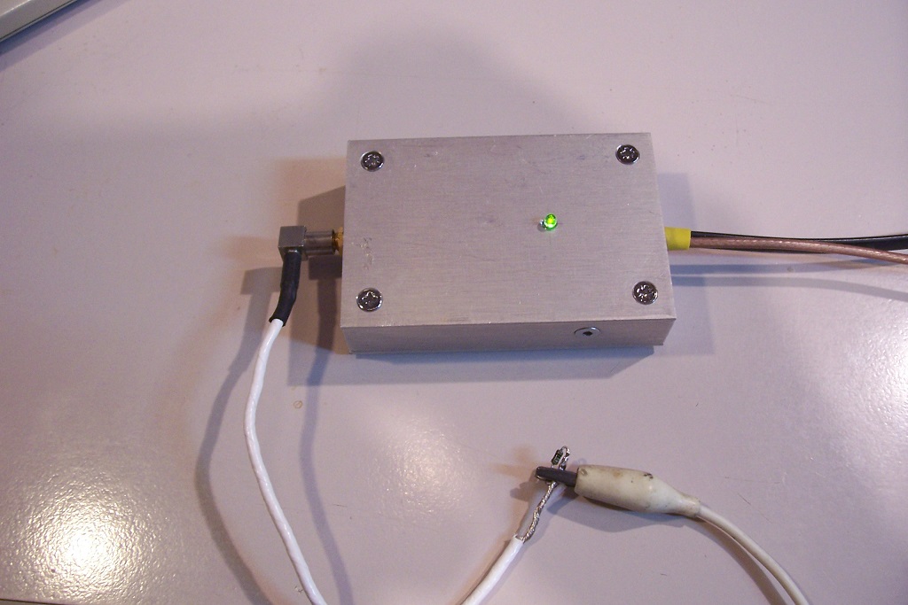
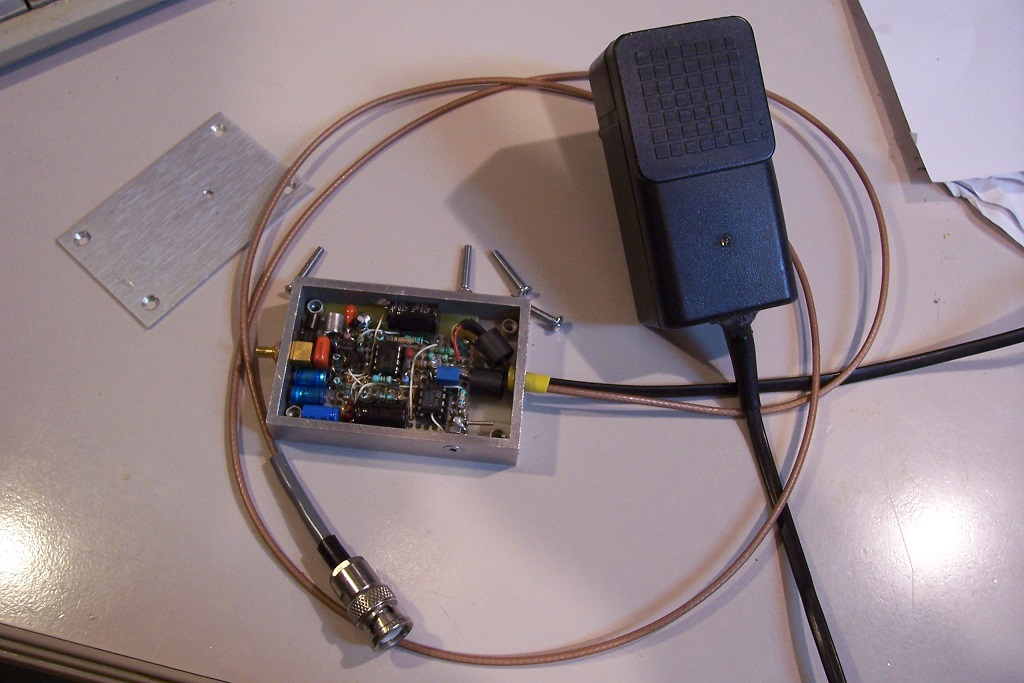
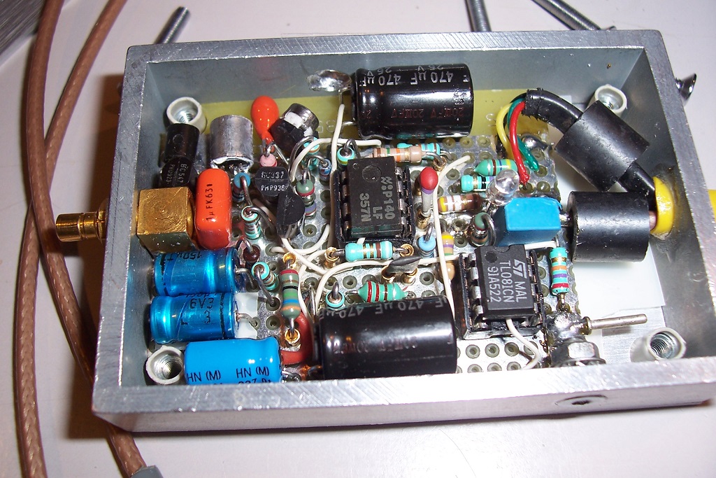
I used Scott's design as a starting point, I added the cascode suggested by Demian to eliminate the effect of the FET's output resistance on the gain and reduce the input capacitance, and I used a CCS/gyrator as a load, to compensate for the low transconductance of older FETs like the J110 without resorting to excessive supply voltages.

I used two separate opamps for the signal and the DC servo, because I wanted to be able to experiment with different types, and the requirements of each function are quite different.
In the end, I opted for a LF357 for the main amp: it is decompensated, which is an advantage here since the effective closed-loop gain is significantly greater than 1, and it has a good slewrate and a clean response.
The DC servo can be any FET or CMOS amplifier.
I used it to reference the output to zero volt, as this is going to be used as a GP lab amplifier.
The servo acts on the CCS rather than directly the FET's gate: meddling with the input made me nervous, and I preferred to add a trimmer for the gate bias, to set the target Id of 20mA.
The range is limited and the adjustment is rather finnicky, but once it is done, it remains reasonably stable.
My bandwidth requirements were 1Hz-->200kHz +/-0.1dB.
In fact, it goes to less than 0.5Hz and to much more than 200kHz: the 3dB bandwidth is 3.5MHz, and that is only because I deliberately limited it, otherwise it could exceed 7MHz, but having a wide bandwidth without necessity is calling for troubles.
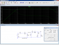
Here is the response with a 2.5Vpp, 200kHz squarewave first attenuated 1K times and then reamplified by the probe.
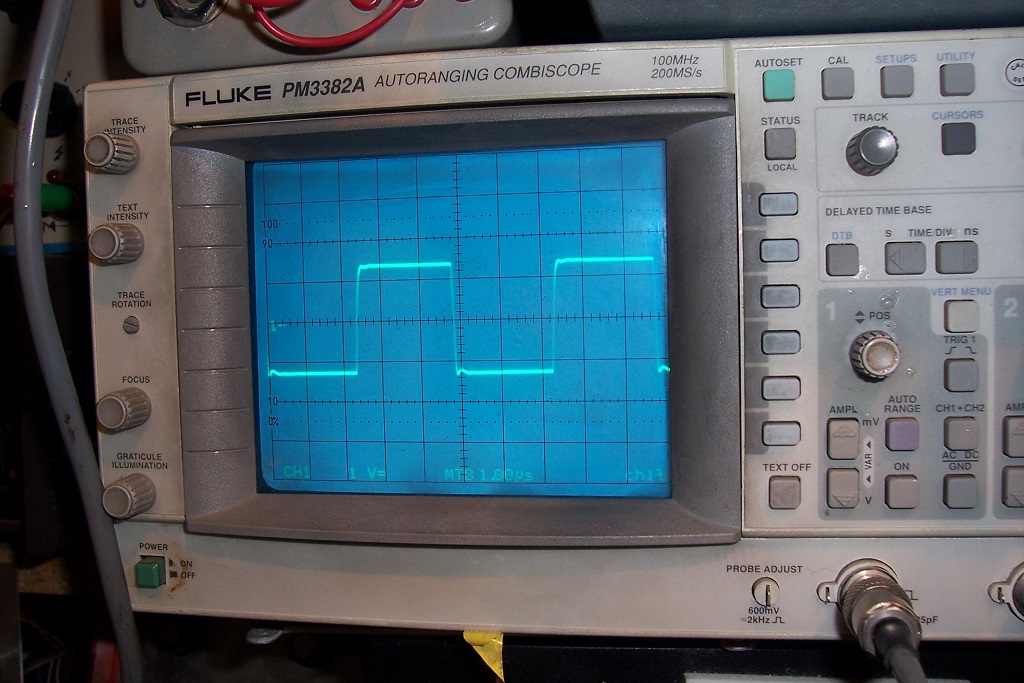
The slight distortion following the transitions is caused by the interaction between the LF357 and the output cable terminated by the oscilloscope (high impedance): when the output changes state, the opamp sees 100 ohm, the series 50 ohm + the cable and has to supply 12.5mA until the reflection from the ~open cable returns.
This causes some perturbations, because 12.5mA is close to what the output is capable of supplying.
With just a 357, terminating the outputs properly is not an option, except for very small signals, and I didn't want to add a buffer, because I am going to use this probe with audio, not video signals
I used Scott's design as a starting point, I added the cascode suggested by Demian to eliminate the effect of the FET's output resistance on the gain and reduce the input capacitance, and I used a CCS/gyrator as a load, to compensate for the low transconductance of older FETs like the J110 without resorting to excessive supply voltages.
I used two separate opamps for the signal and the DC servo, because I wanted to be able to experiment with different types, and the requirements of each function are quite different.
In the end, I opted for a LF357 for the main amp: it is decompensated, which is an advantage here since the effective closed-loop gain is significantly greater than 1, and it has a good slewrate and a clean response.
The DC servo can be any FET or CMOS amplifier.
I used it to reference the output to zero volt, as this is going to be used as a GP lab amplifier.
The servo acts on the CCS rather than directly the FET's gate: meddling with the input made me nervous, and I preferred to add a trimmer for the gate bias, to set the target Id of 20mA.
The range is limited and the adjustment is rather finnicky, but once it is done, it remains reasonably stable.
My bandwidth requirements were 1Hz-->200kHz +/-0.1dB.
In fact, it goes to less than 0.5Hz and to much more than 200kHz: the 3dB bandwidth is 3.5MHz, and that is only because I deliberately limited it, otherwise it could exceed 7MHz, but having a wide bandwidth without necessity is calling for troubles.
Here is the response with a 2.5Vpp, 200kHz squarewave first attenuated 1K times and then reamplified by the probe.
The slight distortion following the transitions is caused by the interaction between the LF357 and the output cable terminated by the oscilloscope (high impedance): when the output changes state, the opamp sees 100 ohm, the series 50 ohm + the cable and has to supply 12.5mA until the reflection from the ~open cable returns.
This causes some perturbations, because 12.5mA is close to what the output is capable of supplying.
With just a 357, terminating the outputs properly is not an option, except for very small signals, and I didn't want to add a buffer, because I am going to use this probe with audio, not video signals
Attachments


Great AC performance. And noise measurements?
You can get a real measure of the input noise by stunting the input with a low value pot or a resistance substituter. Increase the value until the noise increases 3 dB. Then the R equals the equivalent input noise. (You may already be there but I'm sure others will learn from this.) With the gain you have an get app will get a good picture of the noise and online calculators will translate resistance to nV/rtHz.
You can get a real measure of the input noise by stunting the input with a low value pot or a resistance substituter. Increase the value until the noise increases 3 dB. Then the R equals the equivalent input noise. (You may already be there but I'm sure others will learn from this.) With the gain you have an get app will get a good picture of the noise and online calculators will translate resistance to nV/rtHz.
I am sure you are having fun with this. ")
But for me Scott's 1000x LNA is still far simpler to do.
We have built multiple copies and they all worked first time, including a P-JFET version.
If 2SK170 is the problem, then one can use as substitute (just as good if not better) :
2SK369
2SK372
2x 2SK117 GR in parallel
2x 2SK209 GR in parallel
1x 2SK2145 GR (dual) in parallel
The latter two are active and costs << 1USD.
And the articles from Dimitri point to other alternatives.
Measurements Rate SMT Low-Voltage n-JFETs Under Consistent Conditions | Electronic Design
audioXpress December 2018 Addresses Connected Audio Products and Voice Recognition | audioXpress
Cheers,
Patrick
I have already measured it, and it was a very pleasant surprise: @ 1kHz, it came out at 0.77nV/√Hz, and in a 10Hz/10kHz bandwidth, it is 85nV total.Great AC performance. And noise measurements?
I needed to triple check the figures, because I couldn't quite believe them: that is twice better than my expectations: I would have been happy with ~1.5nV. Beating a 2SK170 and going below the 1nV level is something I never dreamed of achieving. Most of it is due to the Teledyne J110, of course, and my crude, preliminary test-jig didn't do justice to its actual performance: it leveled out the results.
Initially, I only tested it to get a complete statistical picture: it was the only one of its kind in my drawer, and I hate relying on a single part, but I ended up using it. If someone else finds these J110's in his stock, he would be well advised to save them preciously, as the gems they are...
You bet I had!I am sure you are having fun with this.
Thanks for the pointers: they will certainly be useful in the future. In the mean time, achieving <1nV using exclusively vintage tech from the seventies was a fun experience.If 2SK170 is the problem, then one can use as substitute (just as good if not better) :
2SK369
2SK372
2x 2SK117 GR in parallel
2x 2SK209 GR in parallel
1x 2SK2145 GR (dual) in parallel
The latter two are active and costs << 1USD.
And the articles from Dimitri point to other alternatives.
Measurements Rate SMT Low-Voltage n-JFETs Under Consistent Conditions | Electronic Design
audioXpress December 2018 Addresses Connected Audio Products and Voice Recognition | audioXpress
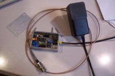
I have now dug out a transformer that is almost the perfect candidate to extend the capabilities of the probe: it has an exact 1:10 ratio, and its secondary magnetizing inductance is 1.5H, meaning the primary is 15mH.
At 10Hz, it translates into ~1ohm, which is a bit low, but anyway for measurements down to ~80pV/√Hz the impedance level needs to be low, and in a 20Hz to 20kHz bandwidth, it should be acceptable.
I will probably modify it slightly though, the primary wire is not as thick as it could be, and this results in a 200mΩ resistance. I only need to add 21 turns on top of the existing windings.
The supplies come from a purpose-built wall-wart.
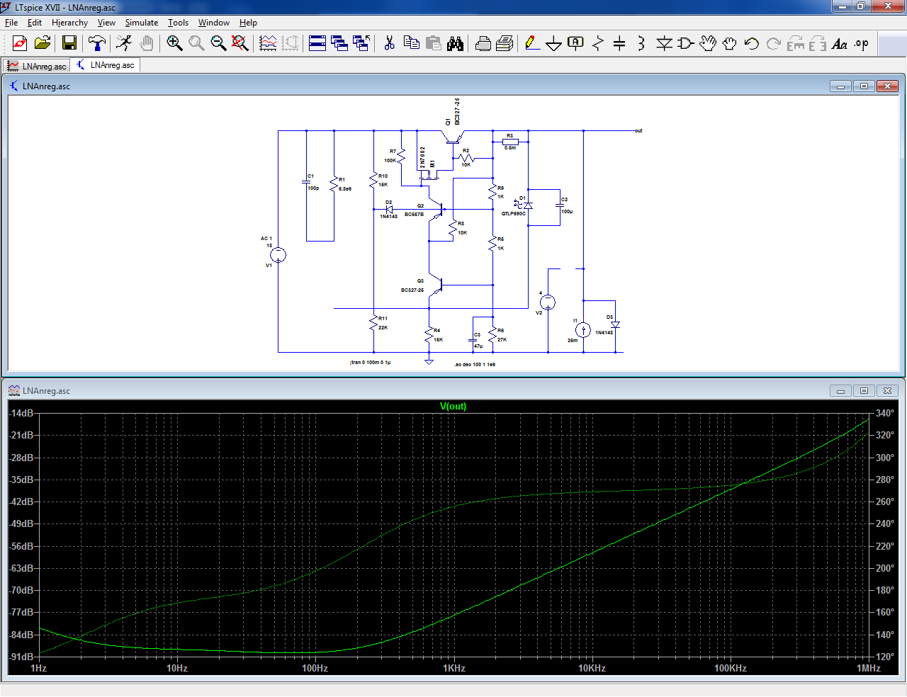
The regulators are variations on the 12-discretes theme:
Just for fun: a superreg with <12 discretes??! ?! ?
Besides being a good real-life test for the concept, they offer low-noise and 90~100dB PSRR, better than a 317 even if it is not actually needed here, and their dropout is somewhat lower, which is important for the negative regulator
They include a few adaptations like the self-starting option: R11,12, D5 for the positive.
The reference LEDs are not even bypassed, and the tweaks to improve the PSRR and output resistance have not been included: the PSRR is sufficient, and the output resistance is relatively unimportant.
Here is the performance of an untweaked regulator:
And here, the Early tweak is active:
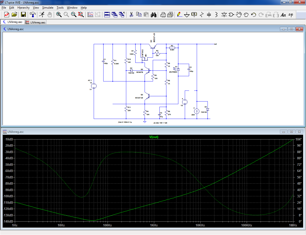
It's just a sim, and has to be taken with a pinch of salt. An improvement of 20dB is realistic
The regulators are variations on the 12-discretes theme:
Just for fun: a superreg with <12 discretes??! ?! ?
Besides being a good real-life test for the concept, they offer low-noise and 90~100dB PSRR, better than a 317 even if it is not actually needed here, and their dropout is somewhat lower, which is important for the negative regulator
They include a few adaptations like the self-starting option: R11,12, D5 for the positive.
The reference LEDs are not even bypassed, and the tweaks to improve the PSRR and output resistance have not been included: the PSRR is sufficient, and the output resistance is relatively unimportant.
Here is the performance of an untweaked regulator:
And here, the Early tweak is active:
It's just a sim, and has to be taken with a pinch of salt. An improvement of 20dB is realistic
Attachments


The input protection presents some challenges: it cannot be dispensed with, because the probe is just another lab accessory, and it will have to cope with gross overloads, live connections/disconnections, coupling capacitors charged to arbitrary voltages, etc., and the gate of the jFET is quite vulnerable.
Usually, input protections rely on a parallel section shunting excessive voltages to the ground, and a series section to limit the fault current, but here, it is impossible to insert any series impedance without degrading the noise performance.
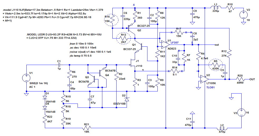
The protection thus relies solely on Q3 and Q4 connected as diodes.
Transistors are more predictable than regular diodes: they have a lower capacitance and leakage current.
Since they are connected to the gate bias source, they operate at a zero bias voltage, thus minimizing the noise current.
The low impedance of C7 completes the AC protection path, and C1 should block DC voltages.
If the DC input voltage is sufficient to cause the breakdown of C1, C7 should melt-down before any damage is done to J1: C7 is a 16V, solid tantalum type.
D2 is an additional safety, in case the meltdown does not happen in time.
All of this may look somewhat paranoiac, but I really want to avoid damaging the FET: I have no replacement, and anyway replacing it would be a nightmare, as it is crimped into a tinned copper clip, itself soldered to the ground plane.
C4 and R6 compensate the negative capacitance generated by the bootstrapping of J1: I want the input impedance to remain well-behaved, even with high impedance sources.
Initially, I had considered an inverse bootstrapping of the drain as it would have resulted in a smaller input capacitance, but finally I opted for the simpler (and probably safer) option of increasing the input capacitance.
For the audio range, a source impedance of up to ~50K is tolerable.
R14 corrects the effect of the finite open-loop gain of the opamp.
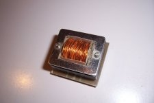
I have now modified the transformer I had found: it is a Siemens V44221 from an old FDM-era instrument.

The result looks messy, because I didn't want to dismantle it to add the turns: the laminations are 0.05mm, very high-perm alloy and disturbing them would do them no good.
I connected the original primary and secondary in series, and managed to add a few more turns to create a 2.2H secondary.
I also wound a new, lower resistance primary.
The primary has a resistance of 90mΩ and the secondary 2.4Ω. They are not perfectly balanced, but they are not going to significantly degrade the noise performance of the probe.
The 22mH of the primary is a bit low, and it will limit the VLF usability, but at noise levels approaching 100pV/√Hz, the source impedance will need to be low anyway.
The whole thing is enclosed in a double mu-metal shield, but even with the high-perm closed magnetic circuit and the shields, it remains sensitive to 50Hz fields.
If I need to use it at the max sensitivity, I will either need to turn off all non-essential equipments, or use a 50Hz notch filter.
A big advantage of a transformer is its galvanic isolation: at these levels, ground loops begin to pose serious problems

I added a small RC to tame the ringing, and the result is quite clean: here are the 100Hz, 1kHz and 10kHz squarewave responses with a 1Ω source:


With the transformer, the input noise becomes 90pV/√Hz, instead of the 77pV theoretical, an acceptable degradation.
Of course, that is not super low: other members do much better, but my goal is to have a usable, low noise preamp to face 99% of my requirements, and I fulfilled it using basically junk-box components.
In case I need record-low levels, I have another transformer, toroidal and much larger which would be sufficient for 100:1 amplification ratio, but currently, <100pV is sufficient for my modest needs
Usually, input protections rely on a parallel section shunting excessive voltages to the ground, and a series section to limit the fault current, but here, it is impossible to insert any series impedance without degrading the noise performance.
The protection thus relies solely on Q3 and Q4 connected as diodes.
Transistors are more predictable than regular diodes: they have a lower capacitance and leakage current.
Since they are connected to the gate bias source, they operate at a zero bias voltage, thus minimizing the noise current.
The low impedance of C7 completes the AC protection path, and C1 should block DC voltages.
If the DC input voltage is sufficient to cause the breakdown of C1, C7 should melt-down before any damage is done to J1: C7 is a 16V, solid tantalum type.
D2 is an additional safety, in case the meltdown does not happen in time.
All of this may look somewhat paranoiac, but I really want to avoid damaging the FET: I have no replacement, and anyway replacing it would be a nightmare, as it is crimped into a tinned copper clip, itself soldered to the ground plane.
C4 and R6 compensate the negative capacitance generated by the bootstrapping of J1: I want the input impedance to remain well-behaved, even with high impedance sources.
Initially, I had considered an inverse bootstrapping of the drain as it would have resulted in a smaller input capacitance, but finally I opted for the simpler (and probably safer) option of increasing the input capacitance.
For the audio range, a source impedance of up to ~50K is tolerable.
R14 corrects the effect of the finite open-loop gain of the opamp.
I have now modified the transformer I had found: it is a Siemens V44221 from an old FDM-era instrument.
The result looks messy, because I didn't want to dismantle it to add the turns: the laminations are 0.05mm, very high-perm alloy and disturbing them would do them no good.
I connected the original primary and secondary in series, and managed to add a few more turns to create a 2.2H secondary.
I also wound a new, lower resistance primary.
The primary has a resistance of 90mΩ and the secondary 2.4Ω. They are not perfectly balanced, but they are not going to significantly degrade the noise performance of the probe.
The 22mH of the primary is a bit low, and it will limit the VLF usability, but at noise levels approaching 100pV/√Hz, the source impedance will need to be low anyway.
The whole thing is enclosed in a double mu-metal shield, but even with the high-perm closed magnetic circuit and the shields, it remains sensitive to 50Hz fields.
If I need to use it at the max sensitivity, I will either need to turn off all non-essential equipments, or use a 50Hz notch filter.
A big advantage of a transformer is its galvanic isolation: at these levels, ground loops begin to pose serious problems
I added a small RC to tame the ringing, and the result is quite clean: here are the 100Hz, 1kHz and 10kHz squarewave responses with a 1Ω source:
With the transformer, the input noise becomes 90pV/√Hz, instead of the 77pV theoretical, an acceptable degradation.
Of course, that is not super low: other members do much better, but my goal is to have a usable, low noise preamp to face 99% of my requirements, and I fulfilled it using basically junk-box components.
In case I need record-low levels, I have another transformer, toroidal and much larger which would be sufficient for 100:1 amplification ratio, but currently, <100pV is sufficient for my modest needs
Attachments


The biggest challenge of the transformer input is the coupling cap in series. It needs to be large, have little leakage and you need to be careful about magnetizing the core. I have a shorting switch on the input to allow for charging the cap. I was using it to measure power supply noise so I had to deal with DC input.
I must be missing something here, but could you explain again how you got 0.77nV/rtHz with a 6nV/rtHz @10Hz jfet (J110)?
https://www.onsemi.com/pub/Collateral/J110-D.PDF
https://www.onsemi.com/pub/Collateral/J110-D.PDF
Last edited:
Hi,
are you sure that you've got the transformer data right?
I was looking for a 100 mH choke yesterday for my chopper to get rid
of the charge injection spikes of my analog switches. The closest thing
I have found at DigiKey was something made by Hammond, weighing in
at 35 pounds, with $10 for each and every pound. That still had 420 mOhm.
I cannot use more capacitance for filtering since that hurts the amplifier input
impedance.
Anything that would fit an even large circuit board was more than 50 Ohms.
Impossible to have two of them in the differential input in front of the
low noise IF amplifier.
24mH 100 mOhm looks about this way:
< http://catalog.triadmagnetics.com/Asset/C-80U.pdf >
< C-80U Triad Magnetics | Induktoren, Spulen, Drosseln | DigiKey >
That thing has two windings, 6 mH@ 50 mOhm each; in the DK product description
they have conveniently chosen the series connection for for the inductance and
the parallel connection for the resistance.
For a transformer, we'd need space and copper for the secondary, too.
For my analog switches, I have found a way to bias them in a way that
minimizes the charge injection, so that it no longer eats my dynamic range.
Just so. The ADG819 spice model gets the injection completely wrong.
cheers, Gerhard
Indeed, and it occurred to me that it could inadvertently turn into a giant CDI system....The biggest challenge of the transformer input is the coupling cap in series. It needs to be large, have little leakage and you need to be careful about magnetizing the core. I have a shorting switch on the input to allow for charging the cap. I was using it to measure power supply noise so I had to deal with DC input.
Also, during my tests, I realized how easy it was to saturate the core: I was making measurements with the signal generator at a comfortable level, with a largish resistor in the output, and when I ventured into low frequencies, the signal showed that the core went in total saturation, despite the series resistor.
My reasoning is that if it is that easy to reach saturation, a moderately higher level should be sufficient to reach the coercitive value.
This means that demagnetizing could be as simple as connecting the transformer to a generator set at 200Hz for example, first at the max amplitude, and then to slowly dial back the level to zero.
Or am I missing something?
I must be missing something here, but could you explain again how you got 0.77nV/rtHz with a 6nV/rtHz @10Hz jfet (J110)?
https://www.onsemi.com/pub/Collateral/J110-D.PDF
The noise density is measured at 1kHz.@ 1kHz, it came out at 0.77nV/√Hz,
That is still better than what the Siliconix datasheet says, but these were among the worst samples I tested: NS were markedly better, but its the Teledyne that really shone
Yes, absolutelyHi,
are you sure that you've got the transformer data right?
100mH is nothing at all, BUT commercial chokes having a low Rdc are intended for high current applications, meaning a large airgap, a lot of iron and a lot of copper to achieve a high saturation threshold.I was looking for a 100 mH choke yesterday for my chopper to get rid
of the charge injection spikes of my analog switches. The closest thing
I have found at DigiKey was something made by Hammond, weighing in
at 35 pounds, with $10 for each and every pound. That still had 420 mOhm.
I cannot use more capacitance for filtering since that hurts the amplifier input
impedance.
A miniature, low resistance inductor could easily be made, but it would only serve niche applications like yours, because it would saturate at values as low as a few mA.
Another parameter to take into account with these power chokes is that their core material is best suited for high induction applications, meaning the initial permeability tends to be low.
For large signal, it is the amplitude permeability that counts.
Materials having a large initial permeability like mumetal only withstand ridiculous induction levels before they saturate
In principle, yes, but in your case you would probably be better using a transformer winding, but not any kind: specifically the 16 ohm secondary of a high-quality tube push-pull output transformer: it will be a good tradeoff between signal-handling and initial inductance.For a transformer, we'd need space and copper for the secondary, too.
It will be costly, but it is off the shelf.
A better solution is to find or modify a high-quality, line level audio transformer, like mine.
Transformers for ribbon microphones or MC cartridges should be good candidates.
With the proper core material, you will be able to reach >0.3H, <0.3 ohm with a size no larger than the one I showed, and it will not require winding a lot of turns.
To check the suitability of a core or transformer, wind a single test turn and measure its inductance: if it is >20µH, it is OK
Another possibility would be to use a large common-mode choke wound on a high permeability ferrite toroid, and to use the windings in series.
With a 47mH one, which is a common value, the total will be ~200mH, with a low DC resistance if it's made to withstand more than a few hundreds mA.
Of course, it will saturate at low currents, but I don't think it is a problem for you.
The basic rule is to respect the V*s product of the core
Here is a suitable example: 2 x 82mH, 150mΩ:
PH9455.826NL Pulse Electronics | Mouser Europe
It will result in a 320mH, 300mΩ inductor and costs 6.65€
Last edited:
The noise density is measured at 1kHz.
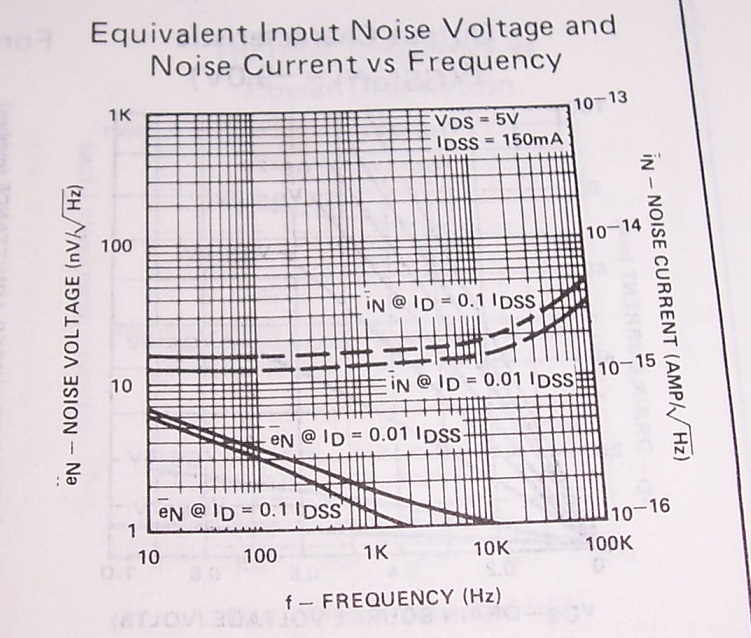
That is still better than what the Siliconix datasheet says, but these were among the worst samples I tested: NS were markedly better, but its the Teledyne that really shone
Ok, so you got an outstanding sample, with noise well under the typical values in the data sheet. Why not using a modern low noise jfet, there are plenty around and cheap as dirt. Even a low noise jfet + bipolar cascode is available (CPH5905 from OnSemi). Granted these are all SMD, but SMD to through hole adapters are available everywhere (for those still shy of soldering the little critters).
Second question, have you checked/measured the low frequency response? I see you have 2 poles and a zero in the servo feedback loop, and as far as I can tell the zero doesn't match a pole, so you may get a significant bump or dip at LF, depending on the pole-zero relative frequency positions.
Third, what are R16 and R13 good for? Q2 can get all the base current it needs from the servo op amp output, and the drain/collector voltage is already set by the U1 op amp non inverting input voltage divider.
Fourth, I find the frequency compensation rather strange and unnecessary complex. A simple lead-lag compensation on the U1 inverting node should be enough and much easier to design and control.
Fifth, while R6/C4 network would certainly work, a small (1-2uH) inducttor with milliohm DC resistance will work as good, if not even better.
Sixth, I don't think you need much of an elaborated power supply for this implementation. The +PSRR is excellent, while the -PSRR can be made arbitrary large by filtering (since the current, short of the opamp, is virtually zero).
Well, I wouldn't say the Teledyne is that much under the datasheet value, firstly because the datasheet pertains to a Siliconix device (I don't have the Teledyne DS), and there is a relatively good agreement there, and the operating gate bias for Id=20mA is -0.3~0.4V, meaning it is not very far from Idss; the curves apply to 0.01 and 0.1*Idss. OK, the influence of Id on noise is relatively marginal, but with a 10 to 1 ratio, there is something to be gained.Ok, so you got an outstanding sample, with noise well under the typical values in the data sheet. Why not using a modern low noise jfet, there are plenty around and cheap as dirt. Even a low noise jfet + bipolar cascode is available (CPH5905 from OnSemi). Granted these are all SMD, but SMD to through hole adapters are available everywhere (for those still shy of soldering the little critters).
Why use vintage devices? The 2SK170 from Scott's version is unobtainable and I would probably get fakes if I ordered them from somewhere, not only in China, and I didn't research alternatives: instead I looked into my (vast) stock, tested a number of devices and stumbled upon that one.
Yes, that was one of my prioritary concern.Second question, have you checked/measured the low frequency response? I see you have 2 poles and a zero in the servo feedback loop, and as far as I can tell the zero doesn't match a pole, so you may get a significant bump or dip at LF, depending on the pole-zero relative frequency positions.
Here is the simulated response: it is quite accurate for the LF response (not for HF, because there are additional real-world equalization measures)
I also attach the sim file, if you want to check by yourself
I designed the CCS/gyrator to operate mostly on its own, but nested within the global loop with just a small correction from the servo, because it reduces the gain of the servo loop.Third, what are R16 and R13 good for? Q2 can get all the base current it needs from the servo op amp output, and the drain/collector voltage is already set by the U1 op amp non inverting input voltage divider.
It minimizes the possible issues of bump and dip you alluded to, and also minimizes servo wind up issues, because of its limited action.
R13 also blunts the raw loop gain available from the opamp + Fet, making the thing more manageable
I servoed the Vcb of the cascode transistor, because of the limited supply voltage: I wanted to make R1 as large as possible, have 6V Vds for J1 and still use an opamp-compatible supply.
Note that I reworked all this many times, and the compromise I found does not satisfy me entirely, because of the two high gain loops cascaded, but that's the best tradeoff I could arrive at without further complexification, and it seems to work well enough in practice
I had different ideas initially, but I evolved this scheme directly on the prototype after selecting the LF357 as main opamp (remember it is decompensated), based on the step-response.Fourth, I find the frequency compensation rather strange and unnecessary complex. A simple lead-lag compensation on the U1 inverting node should be enough and much easier to design and control.
I found that I could get a good step response with this arrangement, but there are certainly alternatives, some of which perhaps better
Yes that's quite possible, but since the response quirk was caused by series impedance (and making it inductive could make it worse to the point of self-oscillation, I didn't explore that route)Fifth, while R6/C4 network would certainly work, a small (1-2uH) inducttor with milliohm DC resistance will work as good, if not even better.
No, I don't think either, but I prefer to remain on the safe side, because you can sometimes have unpleasant surprises.Sixth, I don't think you need much of an elaborated power supply for this implementation. The +PSRR is excellent, while the -PSRR can be made arbitrary large by filtering (since the current, short of the opamp, is virtually zero).
In addition, letting something even so slightly corrupted into the shielding box can sometimes have unexpected effects, just by capacitive coupling.
The same applies to return currents: if the supplies from the wall wart are unclean, the voltage drop along the ground return will make the shielding box non-perfectly neutral wrt. the environment: the supply cable, and the wider mains environment coupled by the capacitance of mains transformer.
As a conclusion, I don't claim this is optimal in any way: it's the version 1.0, and has been designed and built in less than two weeks, meaning there is certainly room for improvement(s).
All I can say is that so far it seems to deliver what it is supposed to, but it is certainly not perfect
Attachments
- Status
- This old topic is closed. If you want to reopen this topic, contact a moderator using the "Report Post" button.
- Home
- Design & Build
- Equipment & Tools
- Sanity-check + end-result: a x 1000 measurement preamplifier