I don't think there is much in the USB space that is high enough spec to do really good measurements
https://www.rme-audio.de/en/products/adi_2-pro.php
Probably the highest spec soundcard around (768k sampling rate
 ), and it's in USB, whether it's worth €1500 is another matter.
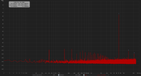
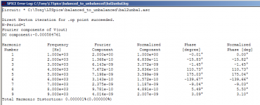
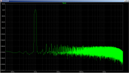
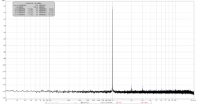
I played with the interface by measuring my head amps. I tried two different setups. First I used diff-to-SE cable (negative signal of the diff. pair is shorted to GND) from the 2i2 out to drive the head amp and SE-to-diff cable from the head amp out to the 2i2 input. As the result I've got a lot of mains harmonics (first attachment).
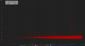
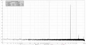
Next I connected differential cable from the 2i2 out to stereo jack of the head amp, so one channel of the head amp receives positive signal of the differential pair and the other channel receives the negative signal of the diff. pair. The stereo output of the head amp drives the diff. input of the interface so the head amp is connected as a differential buffer except that pos. and neg. signals are referenced to the common GND of the stereo headamp. The result is in the second attachment.
The question is if it is reasonable to measure the stereo amp in such a "differential" way. It helps to avoid mains harmonics in the measurement but do I see the true THD of the amp this way? I'm puzzled because I see reduction of the second harmonic in the case of "differential" setup. The third harmonic does not change.
For comparison I also attached SE and differential loopback measurements (third and fourth attachments).
Regards,
Oleg
Attachments

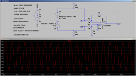
After a long time I am returning to building a balanced to single ended active converter with the gain of 10 to boost the signal from the Focusrite 2i2 output. The sweet spot for the 2i2 output seems to be within the -20dBFS to -15dBFS range (around 0.2V iirc). Thus I assume a gain of 10 is sufficient for my needs. Measurements will be done through the Autoranger designed by Jan Didden which I recently assembled. Before starting with the BAL to SE converter I have a question if I need buffers for the balanced inputs to the converter? According to the specification of 2i2 interface it has 94 Ohm (balanced) output impedance which I assume is simply 47 Ohm in each leg of the BAL output. To me this sounds like I can get away without buffering the inputs and use just one single op-amp for the BAL to SE converter as suggested in post #16 or I better add the buffers?
Regards,
Oleg
Regards,
Oleg
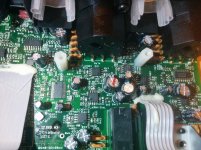
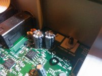
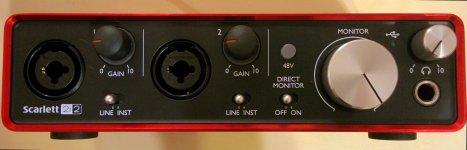
I have finally opened my 2i2 interface. Below are some of my observations:
1. All line inputs and outputs are AC coupled using 47uF 63V (CapXon) polarized capacitors.
2. All inputs and outputs have RF filters.
3. In addition to the NJM4565 op-amps there are two NJM2122 op-amps which probably serve the mic inputs.
4. There are many small Jamicon polarized electrolytic capacitors which purpose I can not easily identify.
5. The op-amps have exactly one decoupling ceramic cap per IC (rail to rail) which together with the electrolytics on all line ins and outs suggests single rail supply. The caps in the PSU are all 16V rated so I assume the supply is around 12VDC.
6. There are three 470uF 16V Yuscon caps which purpose I also can not easily identify but I have a suspicion that they are for unity gain at DC and thus are also in the signal path.
Considering the above, there is a chance to improve the THD at higher signal levels by replacing all polarized electrolytics in signal path by the bi-polar type caps, e.g. Muse series from Nichicon. Also the low supply voltage leaves little headroom for NJM4565 op-amps, so it may be possible to improve things by replacing them with the op-amps less sensitive to the supply voltage level.
If someone is interested in other details related to the inside of the interface just let me know. The interface stays open for a while, so I can easily take pictures and measure connectivity of interesting points.
Regards,
Oleg
Attachments
Hi Oleg, were you planning on doing the circuit 16 but changing it for gain rather than unity (actually it doubles) as it is at the the moment.
Not sure whether this will work well or not. Certainly worth experimenting. I originally used 2K resistors to ensure low noise, but have since found that going higher has very little impact, so maybe going to 10K will be easier on the opamp.
Tony.
Not sure whether this will work well or not. Certainly worth experimenting. I originally used 2K resistors to ensure low noise, but have since found that going higher has very little impact, so maybe going to 10K will be easier on the opamp.
Tony.
Hi Tony,
Yes, the idea was to add some gain to arrive at approx. 2Vrms signal which is needed to test amplifiers at full blast. I thought about making the BAL to SE with 2k resistors and then add a SE gain stage with the gain of 5 followed by 2k linear pot. To realize this I only need to get a potentiometer, the rest I have at hands.
Also an interesting find. The inputs and outputs GND pins are sitting at mid supply which is probably generated by NJM2746 op-amp in MSOP package (the only op-amp which is present in quantity 1 on the entire board and which is sitting between the ins and outs). This suggests that there is no output offset (and I just measured it) to require AC coupling on outputs and inputs since USB power input is galvanically isolated from the onboard power which prevents any possible shorts through external equipment.
Oleg
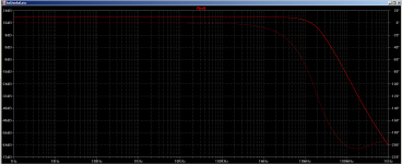
Hi Oleg, I did a sim, and it certainly looks like you can add the gain you want direct to the converter without needing a separate gain stage.
See the attached. It's a great idea, and I will try it myself on my breadboard when I get a chance. 0.2V in 2V out
Real world of course won't be as good as the sim, but the sim indicates that distortion should be minimal.
It sounds like they've created a virtual ground, there must be a dc-dc circuit to as usb only supplies 5V . Will be interested to hear the results of any mods you make!
edit: note also that the 5.6p was to stop some peaking in the sim around 20Mhz (with the original circuit). The version with gain does not have the peaking so I think it could be eliminated.
Tony.
Attachments
Last edited:
Great info, Tony!
The only issue with the added gain is the increase in the noise floor, but since the harmonics level relative to noise should stay the same I guess it won't be too bad. I'm mostly interested in THD rather than THD+N since real noise is impossible to measure with such type of interface.
Anyways, I'll play with this idea and see how far I get with it. I will also try to short the output caps to DC couple the outputs and see if it improves anything. Also, since the line input impedance is 52k I can probably replace the electrolytics at the inputs with 1u~2.2u polyester film caps which fit the lead spacing if AC coupling is a must on this interface. The value of the AC coupling capacitors at the outputs are probably sized such that even if someone connects 600 Ohm loads the low end roll off does not become too severe. But I guess the distortion at low end will skyrocket in this case.
I checked my parts bin and found a couple of LME49990, LME49720, OPA1612 and OPA1642. I guess I will not waste LM49990 on this but am thinking about LME49720 or OPA1612. The datasheet of the OPA1612 suggests that the THD+N at frequencies above 3kHz goes down significantly with added gain (see figs. 7 and 9). I will also try to keep the input impedance low by using 5 times lower resistor values than you used in your simulation, just enough to arrive at 2k load per leg.
Regards,
Oleg
Regards,
Oleg
I'm actually using LM4562's The 49860 in the sim is basically the same. Just having a look at the LME49720 and it looks pretty much identical (from the brief specs on the first page) as the LM4562, so it should work fine
I didn't think about the noise floor. Once I breadboard I will have an idea of what effect there is, as I don't know if the noise floor is limited by the output or the input of the 2i2.
the opa1612 also looks good, and yes it seems it performs better with 2K (or higher I guess) load and gain of 10+
Tony.
Last edited:
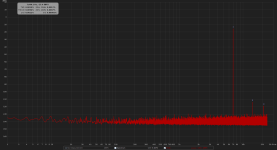
After a bit of testing I can say that electrolytic capacitors at the inputs and outputs are not a problem at all. I tried shorting them (DC coupling) and haven't noticed any change in measured THD and noise floor. I also found a new sweet spot (see attached). The front panel controls are as depicted, the output of the generator is set to -8dBFS in REW, 96kHz sampling rate, balanced loopback connection. This results in measured THD of only 0.00016% which I find very good.
Attachments
Just bought gen 1, How's the test going?
I just measured -8dbFS, it's about 235mV. so that means the maximum input for 2i2 is 560mVrms?
The front panel I just tried, I think it's gain control for pre-amp, turning it up will only add more noise to measurement.
it's blinking red around 560mV, but arta predict around 800mV rms will be peak input.
Dose that mean when I measure noise floor, it will be referring to 800mV?
So -100dBFS will be 8uV?
I did some test with SE, it was miserable. lucky that I saw this thread
Last edited:
- Home
- Design & Build
- Equipment & Tools
- Got Focusrite Scarlett 2i2 (2nd gen) for measurements. What's next?