Fliege 1kHz notch filter project PCB +Twin-T notch PCB
EDIT 1/25/2016 - This thread was just about the Fliege notch filter, but I've added a twin-T notch board in post #62.
*****
The Q401 THD analyzer coming out reminded me about an attempt I made early last year to make a Fliege 1kHz notch filter:
http://www.diyaudio.com/forums/equipment-tools/231401-quantasylum-qa400-17.html#post3821237 (post804)
The notch filter worked quite well, but it also self-oscillated at 100mHz. Oops. I've had the thing on the back burner since then, but just re-did the layout to reduce the opportunity for stray outout-to-input coupling and sent it out to fabrication a couple of days ago. If this one works when it comes back I'll post the Gerbers.
Info on the Fliege notch filter from TI:
www.ti.com/lit/an/slyt235/slyt235.pdf (opens PDF)
www.ti.com/lit/an/sloa096/sloa096.pdf (opens PDF)
Some of the features:
EDIT 1/25/2016 - This thread was just about the Fliege notch filter, but I've added a twin-T notch board in post #62.
*****
The Q401 THD analyzer coming out reminded me about an attempt I made early last year to make a Fliege 1kHz notch filter:
http://www.diyaudio.com/forums/equipment-tools/231401-quantasylum-qa400-17.html#post3821237 (post804)
The notch filter worked quite well, but it also self-oscillated at 100mHz. Oops.
I've had the thing on the back burner since then, but just re-did the layout to reduce the opportunity for stray outout-to-input coupling and sent it out to fabrication a couple of days ago. If this one works when it comes back I'll post the Gerbers. Info on the Fliege notch filter from TI:
www.ti.com/lit/an/slyt235/slyt235.pdf (opens PDF)
www.ti.com/lit/an/sloa096/sloa096.pdf (opens PDF)
Some of the features:
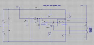
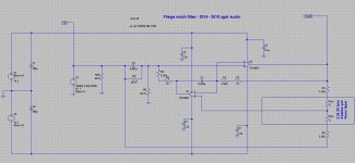
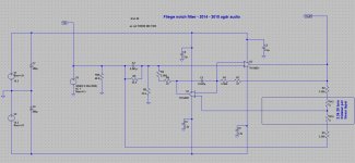
- The Fliege notch filter (which is unity gain) is followed here by an optionally-populated post-amp and current buffer. I have OPA627 (gain of up to 5) and OPA637 (gain of up to 50) penciled in the BOM for the loop op-amp. The post-amplifier can simply be left unpopulated. I have a resistor position (which can also just be a jumper) on the board which bypasses it entirely and runs the filter output directly to the output BNC.
- I have an optional (film) couplng cap and (if you use it) ground return resistor for the OPA6x7 op amp input if someone wishes to block any DC coming in from the source and filter. The OPA6x7 should result in less than 200uV of DC offset (less than 100uV with high grade). I'm using a OPA2140 + BUF634 in another project on the forum and I've measured that at a real-world 47uV.
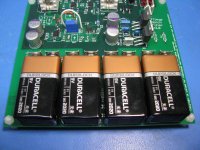
- Can use either the on-board 9V battery clips (2 x 9V = 18Vdc per rail), OR onboard AC supply (16Vac 500mA transformer, WAU16-500), OR an external +/- lab supply. Just populate what you want.
- I've included a regulated power supply using the LT3015 and LT3080. I've used those in another project here on the forum and they work quite well. I'm using the LT3080 instead of the LT1963A because it has a matching 30V maximum input to the LT3015. The 1963A is only 20V. Both vregs are noise bypassed per the data sheets.
- The vregs are adjustable. The BOM parts set them at +/-15.3Vdc since that is the max you can realistically get with a 16Vac transformer and expected line voltage fluctuations.
- I've set the batteries up for two 9V (PP3) on each rail. Depending on how fresh your batteries are that should work out to be 16Vdc - 18Vdc or so. It was tempting to leave off the voltage regulators entirely (be my guest, they are easy enough to simply not populate and jumper accross) since the chips all have absolute maximums of +/-18Vdc, but that little voice of past experience keeps telling me stay at least 1v away from absolute max. I used two batteries per rail under the assumption that higher chip voltages may result is slightly lower THD, rather than just going with the lower 9V per rail (QuantAsylum, I'm looking at you here).
- One of the two "critical" parts are the 0.047uF capacitor. In tight tolerance those are a bit pricey and hard(er) to find in stock. The 1206 COG MLCC 1% I used in last years version is already unobtanium. So I've put three pads in parallel for more options. One is a 1206 for last years's part which I still have a few, a 0805 for a current 1% COG Mouser has in stock, and through-hole pads for a 2% film polypropylene Mouser has right now. The TI white paper on the Fliege in the link notes that in the lab the COG/NPO worked fine but the X7R essentially destroyed the notch quality. Dielectric matters here.
- And the other "critical" part is the 88.7K resistor, another harder to find value. Once again I've hedged by bet with two series resistors. More combinations to add up to the right value, plus adding another 27R in the second position further fine tunes the notch. I've put a 2.5 x 7.2mm through-hole resistor pad in parallel with the 88.7K because Mouser just happens to have two 0.1% 88.7K, for fairly cheap ($1.50 or so) and one is even lower tempco than the SMD thin film (15PPM vs. 25PPM/C).
- I've used the soon-to-be-extinct but excellent LME49990's for the two filter chips.
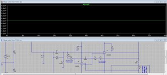
- The schematic has the part number of most everything next to it.
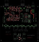
Attachments
-
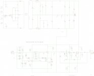 schematic.jpg348.7 KB · Views: 1,257
 -
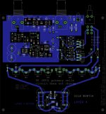 layer 4 V- and route.jpg579.7 KB · Views: 403
 -
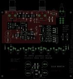 layer 3 V+.jpg788.7 KB · Views: 1,049
 -
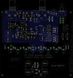 layer 2 ground.jpg823.7 KB · Views: 1,015
 -
 layer 1 route.jpg545.7 KB · Views: 1,070
 -
layout.pdf293.9 KB · Views: 134
-
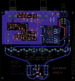 layout.jpg814.4 KB · Views: 1,225
 -
schematic.pdf43.4 KB · Views: 344
Last edited:
Hello agdr,
Good idea to make a PCB for notch filter.
I've build one some year using simple twin-T with opamp as follower(no feedback
to improve Q). Very good results, even if i need to correct manually some
harmonics level to compensate twin-T attenuation at multiple frequency's of fundamental. But my design is in "on the fly way" in small shielded box.
What Q value are you using, and did you have perform some measurements on the filter
to show stop band attenuation (frequency response) ?
Regards.
frex
(For info, i can find easily the Ti AN you have linked, but your links seem broken)
Hi Frex,
Whoops on those links, I'll try again:
http://www.ti.com/lit/an/slyt235/slyt235.pdf
http://www.ti.com/lit/an/sloa096/sloa096.pdf
also a good writeup on Rod Elliot's site:
http://sound.westhost.com/articles/active-filters.htm#s62 (section 6.2)
Those also come up with a Google for "Fliege notch filter".
I also see a typo in what I wrote. The critical resistors are not the 88.7K but rather the 3.36K + 27R. Those are the two I have in series.
The Q should be (88700 / (2 * (3360 + 27))) = 13. One of those articles points out that too high of a Q will result in the notch missing the 2nd harmonic. Good to have a bit of width to the notch, at least through the 2nd. The notch frequency should be (1 / (6.28 * (3360 + 27) * (0.000000047))) = 1000.3 Hz.
I never did actually measure the attenuation or Q on the first one though, just viewed the results as I varied the input Fo. With the 100mHz oscillation I gave up on that one without doing any detailed measuements. But I will on this one, if it works. I'll be curious what the real-world notch depth and Q turns out to be!
As for the oscillation on the last one, I tried several different bypass capacitors and parallel bypass capacitors with no effect. Then I broke one of the feedback loops and it stopped. So I'm fairly certain the 100mHz wasn't from inadequate bypassing but likely output-to-input capacitive coupling via the ground and power planes. I had notched out under the chips. This time I've notched out the planes under the entire feedback network, plus shrunk the trace length a bit. We'll see... I've put test points all over the place on this one to help debug.
I used X7R instead of C0G for the bypass caps. Sergey888 pointed out to me a year or two ago on another project that the impedance vs. frequency curve in the datasheets is actually much better (lower) at 100mHz for the X7R.
Last edited:
Hello again agdr,
I've read the Ti's apps note, and this type of notch filter seem to be interesting,
particularly because tuning is much easier. Also not much parts needs to be paired.
Maybe the concern would be that the feedback OPAMP of the filter needs to be well chosen.
It must have high bandwidth, slew-rate and low THD, because it will try to reproduce same signal as the input, with opposite phase in order to cancel it.
This is for same reason that i've used a Twint-T filter without feedback.
Feedback allow high Q, but produce lower notch attenuation and can produce itself THD that can re-injected to output filter.
The design use a passive Twin-T and a simple OPAMP as follower (OPA134).
Because signal level at input and output of the opamp is very low (mV range),
the opamp follower doesn't introduce any THD in the whole filter.
Of course, there is an disadvantage; you need to correct the harmonics level
of your measurement because at Q=1 the filter introduce some attenuation
outside the notch frequency.
You can show HERE the measurement plot of my filter, that i've used to check the
THD level of the AN67 10kHz ultrapure sine oscillator (to -168 dBc !).
Regards.
Frex
Turbon - yep it is the latter, 100MHz. Lol, my nomenclature there has given Sergery888 a headache too in the past (millihertz).
Frex - Hey nice Twin-T filter there!
The op amp choice for the Fliege does sound pretty critical. It has to be unity gain stable (which the LME49990 is) since the Fliege filter is unity gain. On page 24 of that first TI app note, under "results at 10KHz", he says "The bad news is that to escape op amp bandwidth limitations, the highest notch frequency possible with a 100MHz op amp is somewhere between 10 and 100KHz". The LME49990 has a 110MHz GBP. With any luck it should be good for both 1KHz and 10KHz notches, and probably up to 20KHz without any significant notch degredation.
The LME49990 also has fairly high slew, for audio band use anyway, and vanishingly low THD. The 49990 is the chip that opc uses in his "Wire" line of DIY headamps here. He has made AP THD+N measurements on the result and it looks fantastic. The chip is fairly low noise at 1.3nV/(sqrt(HZ) at F=1KHz. I'll be quite curious to see how much noise the chips add to he signal.
On the notch frequency I forgot to say that with the 1% tolerance of the 0.047uF "set" caps that gives about +/-10Hz in either direction, 990Hz to 1010Hz. But on p22 in the TI app note he says the pot is good for a 1% frequency correction while maintaining a 100:1 rejection. So the pot may be able to more-or-less compensate for any notch frequency shift from the "set" capacitor tolerance.
In the TI papers it sounds like at that point in time even 0.010uF C0Gs were not available. He was forced to use 0.001uF C0G MLCC and adjust the resistor accordingly. Now we have 0.047uF C0G's!
The thing I worried about the most in the design is the effect of output coax cable capacitance. The LME49990 is only good for 100pF on the output without using an isolating resistor, which is why the resistor in series if the post-amp is bypassed. It is still not clear to me if output capacitance (without the series output isolating resistor) would de-tune the filter notch, given the design of the Fliege. But with the post-amplifier I looped the OPA6x7 around a SMD BUF634. The result should be able to drive just about any reasonable length of coax cable without any series resistors. The OPA627 is unity gain stable (but not the uncompensated 637 for vgains over 5) so there should be no reason why that post-amp couldn't simply be run with a votlage gain of 1x as a coax-cable-driving current buffer.
Last edited:
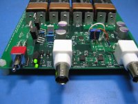
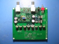
PC board back - input *requires* a resistor to ground
The PC board for this Fliege notch filter project came back a few days ago and I've built it up. Well... I can see this one is going to take some troubleshooting. I'll post some photos later. But I have made one discovery already here regarding output DC.
The battery terminals, power supply (voltage regulators), and post-amplifier loop onthe board all work fine.
So far I have the Fliege filter section disconnected from the post-filter-amplifier by leaving the J7 jumper off (filter-to-amplifier feed) and R28 off (amplifier-to-output feed). That allows me to isolate and troubleshoot just the Fliege filter section itself.
The first thing I discovered on testing was -12.7Vdc on the filter output. This is with the filter-to-output-BNC capacitance isolation resistor R18 (was 20R at the time, now 49.9R, see below) installed. -12.7 is essentially the LME49990 output at the negative rail, with the +/-15.3vdc supplies. I have to admit that in all the LTSpice sims I did of this filter I never really paid attention to the output DC, other than it seemed to be somewhere around 0V as expected.
My first instinctive thing to try was grounding the input BNC. Sure enough that did it. The -12.7Vdc on the output went down to -4mVdc, roughly the expected level since that is around the input offset voltage of the LME49990, plus various voltage drops in the input resistors with small currents going through them. Hmmm. So then I tried successively higher values of resistors (input BNC to ground) in place of input grounding and discovered that any resistor up to around 100K would result in -5mV or so output. Greater than 100K the output started creeping up rather quickly. Adding the input resistor turned out to be easy because I had left a space ground hole JP13 near the input BNC and a hole on the input line, JP5.
With that experimental info I went back to the TI article on the Fliege notch filter
http://www.ti.com/lit/an/slyt235/slyt235.pdf (opens PDF)
and read through again. The schematic in there shows no input resistor to ground at all. BUT... on the re-read I realized they had built the thing up on a THS4032 evaluation board by doing some cut and jumpers and part substitutions. I looked up a THS4032 eval board
http://www.ti.com/lit/pdf/slou039 (opens PDF)
and sure enough, 50 ohm input-to ground resistors on each half (a dual chip) AND 50 ohm series resistor to output. They chose 50 ohm to properly (resistively, no reflections) terminate the 50 ohm coax. That explains the missing input-to-ground resistor, it was already on the eval board and they didn't bother to show it on their Fliege notch filter schematic. Turns out that eval board is pre-configured as two non-inverting amplifiers.
I changed the added input resistor on mine to 49.9R and bumped the output resistor R18 up to 49.9R to match what their eval board had. DC output problem solved. -3mV or so on the output now.
So the bottom line in all of this: if anyone is trying to re-create the Fliege notch filter circuit in the TI app note linked above, you need a not-shown resistor to ground on the input or you will have substantial DC on the output.
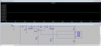
I was curious as to exactly why, from a circuit standpoint, the input resistor is needed. Back to LTspice, plots below.
* The first plot shows the DC result at the Fliege notch filter output with the input voltage source completely removed and a 50R resistor to ground added at the input (0 Hz, of course). The notch filter output is around -6mVdc, a reasonable match to the real-world -3mV I'm measuring.
* The next plot is the same, but with a 100K input resistor instead of 50R. The output DC goes down slightly to -8mVdc.
* Next is with a 1 meg input. Output now around -73mVdc
* Next with a 100 meg input and resulting large jump to around -7.2Vdc output.
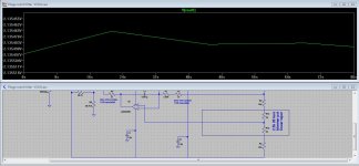
* and finally 500 meg, resulting in pegging the negative rail at -15Vdc. Now just the obvious caution here, this is Spice, so 500 meg resistors work just great, lol. In the real measurements around 5 meg would hit the rail at -12.7Vdc.
And a couple of more that help show what is going on. These have the same lack of input signal and 500meg input resistor as the last plot, but now I'm varying the two resistors on the output of the 2nd op-amp in the Fliege notch filter (with their mid-point going to the non-inverting input of the second op-amp). In my Spice sim here those are R2 and R3. In TI's first Fliege paper they have those as both 1K. In their second paper online they are 100K. In all the plots above I have listed so far those two are the value I soldered in teh actual board, the same value as the "set" resistors, 3.36K with the 50R pot set in the middle.
* The next plot shows the DC result with the 500 meg input resistor but the two output resistors now set to 10K. The output rises from the -15Vdc rail to around -2.1Vdc. So the output DC is heading back toward the middle (toward 0V).
* The final plot shows the DC result with the two output resistors now set to 100K. A complete output DC flip! +15V rail now instead of the -15Vdc rail.
The feedback loop(s) are causing the 2nd op-amp output to peg at one rail or the other, depending on the voltage divider formed between the two output resistors and that new input-to-ground resistor.
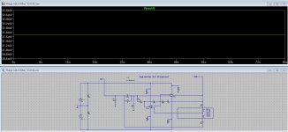
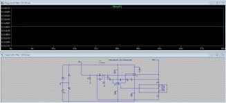
So that is the DC problem solved. The filter oscillates again at around 3MHz. Before blaming inductance in overly-long PC traces and via holes (which it may be) I'm going to try different op amps. I have a pair of the THD4031's in the TI article on order. They have a much higher slew and much higher output current, which may make a difference. Will be interesting to see!
I've also determined from the Mouser listings that 0805-sized SMD 22nF C0G MLCC caps are in fairly good stock, as are (of course) 10nF, as an alternative to the 47nF (the notch frequency "set" capacitors) that I'm using here. I liked the 47nF because it resulted in smaller value notch frequency set resistors of 3.36K + 27R, to keep Johnson noise low, but still high enough not to cause a current drive problem for the LME49990. Going to the lower value "notch frequency set" capacitors results in higher value "set" resistors, but still not too bad. I think one was around 7.23K total and the other around 15.8K total as I recall.
The PC board for this Fliege notch filter project came back a few days ago and I've built it up. Well... I can see this one is going to take some troubleshooting.
I'll post some photos later. But I have made one discovery already here regarding output DC.The battery terminals, power supply (voltage regulators), and post-amplifier loop onthe board all work fine.
So far I have the Fliege filter section disconnected from the post-filter-amplifier by leaving the J7 jumper off (filter-to-amplifier feed) and R28 off (amplifier-to-output feed). That allows me to isolate and troubleshoot just the Fliege filter section itself.
The first thing I discovered on testing was -12.7Vdc on the filter output.
This is with the filter-to-output-BNC capacitance isolation resistor R18 (was 20R at the time, now 49.9R, see below) installed. -12.7 is essentially the LME49990 output at the negative rail, with the +/-15.3vdc supplies. I have to admit that in all the LTSpice sims I did of this filter I never really paid attention to the output DC, other than it seemed to be somewhere around 0V as expected.My first instinctive thing to try was grounding the input BNC. Sure enough that did it. The -12.7Vdc on the output went down to -4mVdc, roughly the expected level since that is around the input offset voltage of the LME49990, plus various voltage drops in the input resistors with small currents going through them. Hmmm. So then I tried successively higher values of resistors (input BNC to ground) in place of input grounding and discovered that any resistor up to around 100K would result in -5mV or so output. Greater than 100K the output started creeping up rather quickly. Adding the input resistor turned out to be easy because I had left a space ground hole JP13 near the input BNC and a hole on the input line, JP5.
With that experimental info I went back to the TI article on the Fliege notch filter
http://www.ti.com/lit/an/slyt235/slyt235.pdf (opens PDF)
and read through again. The schematic in there shows no input resistor to ground at all. BUT... on the re-read I realized they had built the thing up on a THS4032 evaluation board by doing some cut and jumpers and part substitutions. I looked up a THS4032 eval board
http://www.ti.com/lit/pdf/slou039 (opens PDF)
and sure enough, 50 ohm input-to ground resistors on each half (a dual chip) AND 50 ohm series resistor to output. They chose 50 ohm to properly (resistively, no reflections) terminate the 50 ohm coax. That explains the missing input-to-ground resistor, it was already on the eval board and they didn't bother to show it on their Fliege notch filter schematic. Turns out that eval board is pre-configured as two non-inverting amplifiers.
I changed the added input resistor on mine to 49.9R and bumped the output resistor R18 up to 49.9R to match what their eval board had. DC output problem solved.
-3mV or so on the output now.So the bottom line in all of this: if anyone is trying to re-create the Fliege notch filter circuit in the TI app note linked above, you need a not-shown resistor to ground on the input or you will have substantial DC on the output.
I was curious as to exactly why, from a circuit standpoint, the input resistor is needed. Back to LTspice, plots below.
* The first plot shows the DC result at the Fliege notch filter output with the input voltage source completely removed and a 50R resistor to ground added at the input (0 Hz, of course). The notch filter output is around -6mVdc, a reasonable match to the real-world -3mV I'm measuring.
* The next plot is the same, but with a 100K input resistor instead of 50R. The output DC goes down slightly to -8mVdc.
* Next is with a 1 meg input. Output now around -73mVdc
* Next with a 100 meg input and resulting large jump to around -7.2Vdc output.
* and finally 500 meg, resulting in pegging the negative rail at -15Vdc. Now just the obvious caution here, this is Spice, so 500 meg resistors work just great, lol.
In the real measurements around 5 meg would hit the rail at -12.7Vdc.And a couple of more that help show what is going on. These have the same lack of input signal and 500meg input resistor as the last plot, but now I'm varying the two resistors on the output of the 2nd op-amp in the Fliege notch filter (with their mid-point going to the non-inverting input of the second op-amp). In my Spice sim here those are R2 and R3. In TI's first Fliege paper they have those as both 1K. In their second paper online they are 100K. In all the plots above I have listed so far those two are the value I soldered in teh actual board, the same value as the "set" resistors, 3.36K with the 50R pot set in the middle.
* The next plot shows the DC result with the 500 meg input resistor but the two output resistors now set to 10K. The output rises from the -15Vdc rail to around -2.1Vdc. So the output DC is heading back toward the middle (toward 0V).
* The final plot shows the DC result with the two output resistors now set to 100K. A complete output DC flip! +15V rail now instead of the -15Vdc rail.
The feedback loop(s) are causing the 2nd op-amp output to peg at one rail or the other, depending on the voltage divider formed between the two output resistors and that new input-to-ground resistor.
So that is the DC problem solved. The filter oscillates again at around 3MHz. Before blaming inductance in overly-long PC traces and via holes (which it may be) I'm going to try different op amps. I have a pair of the THD4031's in the TI article on order. They have a much higher slew and much higher output current, which may make a difference. Will be interesting to see!
I've also determined from the Mouser listings that 0805-sized SMD 22nF C0G MLCC caps are in fairly good stock, as are (of course) 10nF, as an alternative to the 47nF (the notch frequency "set" capacitors) that I'm using here. I liked the 47nF because it resulted in smaller value notch frequency set resistors of 3.36K + 27R, to keep Johnson noise low, but still high enough not to cause a current drive problem for the LME49990. Going to the lower value "notch frequency set" capacitors results in higher value "set" resistors, but still not too bad. I think one was around 7.23K total and the other around 15.8K total as I recall.
Attachments
-
 500meg input 0Hz 2x100K out.JPG135.3 KB · Views: 138
 -
 500meg input 0Hz 2x10K out.JPG140.5 KB · Views: 149
 -
 500meg input 0Hz.JPG142.1 KB · Views: 101
 -
 100meg input 0Hz.JPG137.8 KB · Views: 94
 -
 1meg input 0Hz.JPG133 KB · Views: 110
 -
 100K input 0Hz.JPG132.9 KB · Views: 205
 -
 50R input 0Hz.JPG134.3 KB · Views: 222
Last edited:
Hi Frex,
Good thought! I've included the full LTSpice schematic below. That 500 meg input-to-ground resistor is 49.9 ohm on the board.
After I did the post I discovered a mistake on the Spice schematic. I still had the two power supply voltage sources at 18V (for two 9V batteries on each rail with no voltage regulator). That is why the "pinned to the rail" voltage on the op-amp outputs were simulating at around +/-15V vs. the real-world measured 12.7Vdc. I've changed the voltage sources to 15.3Vdc now to match the voltage regulator outputs. The simulated op-amp "pinned" outputs are now a closer-match at +/- 11.7Vdc or so.
Regarding the op-amp input bias current, the datasheet for the LME49990 lists 30nA typical, but 500nA maximum. From the schematic I'm assuming that for U1 the input bias current gets sourced/sunk through both the 88.7K R6 to ground and the 3.36K R4 to the U2 output. Assuming worst-case, with the 0.5uA bias current, through the 88.7K would produce a drop (and input voltage) of 44mV, if I've done the math right.. But that is in parallel with the 3.36K. I'm not exactly sure how to calculate the drop on that one since it returns to the output of U2, which should be varying. More thought required.
So you are right, that input bias current deserves some thought. If the swap to the THS4032 doesn't produce any interesting results maybe trying FET-input op-amps would be worth a shot.
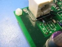
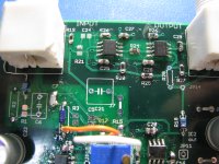
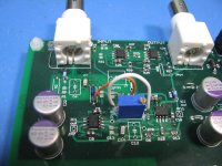
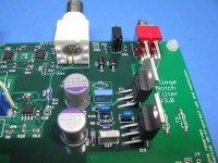
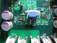
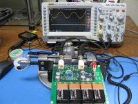
Below are photos of the board. The two jumpers around the trimpot are attempts to track down the oscillation. There is a trace that goes under the pot I was suspicious about (input to output capacitive coupling), but cutting it at both ends and jumpering made no difference.
With the other jumper I've turned one of the 0805 SMD 3.36K resistors 90 degress to unhook it from one pad. Then I jumpered the unhooked end to ground. That is the 3.36K that is in series with the trimpot, on the bottom. By grounding that resistor and removing one of the 88.7K resistors (which I also did) the Fleige notch circuit reverts to a Fliege high pass filter circuit. In the link to Rod Elliot's site here
http://sound.westhost.com/articles/active-filters.htm
in section 7.1 he also has the schematics of a Fliege low and high pass filter, which get combined to make the notch filter. My thinking was to eliminate one feedback loop, just reverting to the high pass filter, to see if that stopped the oscillation. It didn't, unfortunately.
The next to the last photo shows the new input-to-ground resistor I added, near the side of the input BNC. The missing "R2" in that photo is the 88.7K "Q set" resistor I've temporarily removed, along with adding the 3.36K jumper to ground to convert it into the Fliege high pass filter.
I'm still puzzled a bit as to why the two 88.7K "Q set" resistors don't seem to work as adequate input-to-ground resistors, even though they are in parallel with the input (to ground). at 0 Hz (DC analysis so C2 isn't a factor) it appears to be cascaded voltage dividers feeding the non-inverting input of U1. The 3.36K output resistors and pot first in series with the input resistor to ground (if added) for the first division. Then that output voltage applied across the 88.7Ks for a second division.
If I wind up doing another board spin I'm going to use a dual chip like the TI app note's THS4032 and dramatically shorten the traces, leaving out the various alternative part package options. Then add some ground polygons on the top feeding the bypass caps and nailing those polygons to the interior ground layer with a whole bunch of vias to keep the inductances low(er). via inductance to the interior 2nd-layer ground trace may be one of the culprits.
Good thought! I've included the full LTSpice schematic below. That 500 meg input-to-ground resistor is 49.9 ohm on the board.
After I did the post I discovered a mistake on the Spice schematic. I still had the two power supply voltage sources at 18V (for two 9V batteries on each rail with no voltage regulator). That is why the "pinned to the rail" voltage on the op-amp outputs were simulating at around +/-15V vs. the real-world measured 12.7Vdc. I've changed the voltage sources to 15.3Vdc now to match the voltage regulator outputs. The simulated op-amp "pinned" outputs are now a closer-match at +/- 11.7Vdc or so.
Regarding the op-amp input bias current, the datasheet for the LME49990 lists 30nA typical, but 500nA maximum. From the schematic I'm assuming that for U1 the input bias current gets sourced/sunk through both the 88.7K R6 to ground and the 3.36K R4 to the U2 output. Assuming worst-case, with the 0.5uA bias current, through the 88.7K would produce a drop (and input voltage) of 44mV, if I've done the math right.. But that is in parallel with the 3.36K. I'm not exactly sure how to calculate the drop on that one since it returns to the output of U2, which should be varying. More thought required.
So you are right, that input bias current deserves some thought. If the swap to the THS4032 doesn't produce any interesting results maybe trying FET-input op-amps would be worth a shot.
Below are photos of the board. The two jumpers around the trimpot are attempts to track down the oscillation. There is a trace that goes under the pot I was suspicious about (input to output capacitive coupling), but cutting it at both ends and jumpering made no difference.
With the other jumper I've turned one of the 0805 SMD 3.36K resistors 90 degress to unhook it from one pad. Then I jumpered the unhooked end to ground. That is the 3.36K that is in series with the trimpot, on the bottom. By grounding that resistor and removing one of the 88.7K resistors (which I also did) the Fleige notch circuit reverts to a Fliege high pass filter circuit. In the link to Rod Elliot's site here
http://sound.westhost.com/articles/active-filters.htm
in section 7.1 he also has the schematics of a Fliege low and high pass filter, which get combined to make the notch filter. My thinking was to eliminate one feedback loop, just reverting to the high pass filter, to see if that stopped the oscillation. It didn't, unfortunately.
The next to the last photo shows the new input-to-ground resistor I added, near the side of the input BNC. The missing "R2" in that photo is the 88.7K "Q set" resistor I've temporarily removed, along with adding the 3.36K jumper to ground to convert it into the Fliege high pass filter.
I'm still puzzled a bit as to why the two 88.7K "Q set" resistors don't seem to work as adequate input-to-ground resistors, even though they are in parallel with the input (to ground). at 0 Hz (DC analysis so C2 isn't a factor) it appears to be cascaded voltage dividers feeding the non-inverting input of U1. The 3.36K output resistors and pot first in series with the input resistor to ground (if added) for the first division. Then that output voltage applied across the 88.7Ks for a second division.
If I wind up doing another board spin I'm going to use a dual chip like the TI app note's THS4032 and dramatically shorten the traces, leaving out the various alternative part package options. Then add some ground polygons on the top feeding the bypass caps and nailing those polygons to the interior ground layer with a whole bunch of vias to keep the inductances low(er). via inductance to the interior 2nd-layer ground trace may be one of the culprits.
Attachments
-
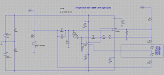
 schematic.jpg170.3 KB · Views: 217
 -
 IMG_3898.JPG600.8 KB · Views: 136
 -
 IMG_3897.JPG583.8 KB · Views: 104
 -
 IMG_3896.JPG637 KB · Views: 104
 -
 IMG_3894.JPG585.3 KB · Views: 113
 -
 IMG_3893.JPG598.3 KB · Views: 148
 -
 IMG_3892.JPG673 KB · Views: 166
 -
 IMG_3890.JPG642.8 KB · Views: 160
 -
 IMG_3889.JPG595.5 KB · Views: 151
 -
 IMG_3888.JPG679.7 KB · Views: 221
Last edited:
It works perfectly with the THS4031 chips!
I found the oscillation problem! It was, in fact, some issue with the LME49990 chips. The THS4031 (single version of the THS4032 in the TI app note) arrived from Mouser today. I swapped out the LME49990s for the THS4031's and it works absolutely perfectly. Zero oscillation across the spectrum - photos below. The 1KHz notch also works just exactly as expected, more photos below.
Since it works I'll go ahead and post the Gerbers and BOM for this project in a couple of days once I get the BOM cleaned up a bit.
So if anyone out there has some insight into why the LME49990 bombs in this application, please share! I need to compare the datasheets in more detail, but at a minimum the slew and output current of the THS4031 is vastly greater. If it isn't one of those I would be suspicious of output capacitance driving problems with the LME part (or capacitance on the input problems). There is a weird hit-and-run sort of section in the LME49990 datasheet about adding an optional series LCR network to the output, but they are extremely vauge as to when or why. National apparently knew of some problem there they didn't want to expand on. I haven't had any problem with the chip in other projects I've posted here, but those are all bandwidth limited headphone amplifiers with the typical non-inverting configuration.
At any rate, here are some photos:
* Several things going on in the first photo, 3899. I've swapped both LME49990's with the THS4031. I've re-installed the two 88.7K 0.1% through hole "Q set" resistors R2 and R4 that I had removed to convert it temporarily to a high pass filter. So it is back to a Fliege notch filter with a Q of 13. And same with the orange jumper wire from the last post. That is removed and the 3.36K 0805 resistor is rotated and soldered again on the pads. Just a reminder that the empty SMD pads and through-holes on the board are for optional alternate packages for the "set" resistors and capacitors, as noted on the schematic and BOM. Just provides more flexibility on finding tight-tolerance parts in stock at Mouser or Digikey.
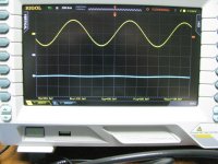
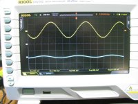
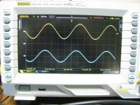
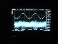
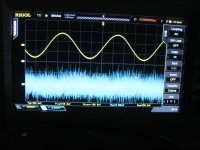
* the second photo 3901 shows the test setup. The top yellow trace is the signal generator, set for 500mV p-p (scope on both traces set for 200mV/div). That source is BNC T'ed and feeds the Fliege notch board via the left BNC. The bottom blue trace is the Fliege notch ouput via the righthand board BNC.
* next photo 3902 shows 1.000KHz. Good! Notched right out.
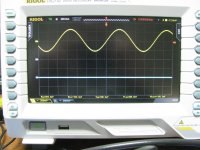
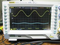
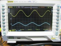
* The next two photos 3904 and 3909 show 1.0010KHz and 999.0Hz. I'm posting the results on both sides of the test signal here to show the symmetry of the notch well. Just a very slight ripple out of the notch filter on the 200mV scope setting.
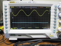
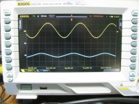
* Next two 3905 and 3910 are 1.0050KHz and 995.0Hz.
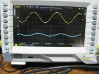
* Next two 3906 and 3911 are 1.0100KHz and 990.0Hz
I found the oscillation problem!
It was, in fact, some issue with the LME49990 chips. The THS4031 (single version of the THS4032 in the TI app note) arrived from Mouser today. I swapped out the LME49990s for the THS4031's and it works absolutely perfectly. Zero oscillation across the spectrum - photos below. The 1KHz notch also works just exactly as expected, more photos below.Since it works I'll go ahead and post the Gerbers and BOM for this project in a couple of days once I get the BOM cleaned up a bit.
So if anyone out there has some insight into why the LME49990 bombs in this application, please share! I need to compare the datasheets in more detail, but at a minimum the slew and output current of the THS4031 is vastly greater. If it isn't one of those I would be suspicious of output capacitance driving problems with the LME part (or capacitance on the input problems). There is a weird hit-and-run sort of section in the LME49990 datasheet about adding an optional series LCR network to the output, but they are extremely vauge as to when or why. National apparently knew of some problem there they didn't want to expand on. I haven't had any problem with the chip in other projects I've posted here, but those are all bandwidth limited headphone amplifiers with the typical non-inverting configuration.
At any rate, here are some photos:
* Several things going on in the first photo, 3899. I've swapped both LME49990's with the THS4031. I've re-installed the two 88.7K 0.1% through hole "Q set" resistors R2 and R4 that I had removed to convert it temporarily to a high pass filter. So it is back to a Fliege notch filter with a Q of 13. And same with the orange jumper wire from the last post. That is removed and the 3.36K 0805 resistor is rotated and soldered again on the pads. Just a reminder that the empty SMD pads and through-holes on the board are for optional alternate packages for the "set" resistors and capacitors, as noted on the schematic and BOM. Just provides more flexibility on finding tight-tolerance parts in stock at Mouser or Digikey.
* the second photo 3901 shows the test setup. The top yellow trace is the signal generator, set for 500mV p-p (scope on both traces set for 200mV/div). That source is BNC T'ed and feeds the Fliege notch board via the left BNC. The bottom blue trace is the Fliege notch ouput via the righthand board BNC.
* next photo 3902 shows 1.000KHz. Good! Notched right out.
* The next two photos 3904 and 3909 show 1.0010KHz and 999.0Hz. I'm posting the results on both sides of the test signal here to show the symmetry of the notch well. Just a very slight ripple out of the notch filter on the 200mV scope setting.
* Next two 3905 and 3910 are 1.0050KHz and 995.0Hz.
* Next two 3906 and 3911 are 1.0100KHz and 990.0Hz
Attachments
-
 IMG_3899.JPG694.1 KB · Views: 152
 -
 IMG_3901.JPG664.9 KB · Views: 170
 -
 IMG_3904.JPG523.5 KB · Views: 113
 -
 IMG_3903.JPG500.1 KB · Views: 148
 -
 IMG_3909.JPG567.3 KB · Views: 86
 -
 IMG_3905.JPG496.8 KB · Views: 96
 -
 IMG_3910.JPG533.4 KB · Views: 95
 -
 IMG_3906.JPG514.2 KB · Views: 107
 -
 IMG_3911.JPG510.9 KB · Views: 101
Last edited:
Fliege 1KHz notch filter test results, part 2
Continuing from the above post (ran out of photo slots)..
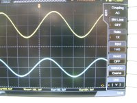
* 3907 and 3908 are 1.0200KHz and 1.0500KHz. I didn't take photos of the other side of the notch at the 20 and 50Hz variation unfortunately.
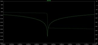
* 3912 shows the -3dB point, if I did my math on that correctly, and it occured at 1.0400KHz. The scope has the peak of the signal reported below the trace at 264V. I varied the source frequency to set the peak of the output (blue) to 184mV, which is as close as I could get it to 186mV. Unfortunately the scope's measurement kept bouncing back and forth between 184mV and 192mV. Looks like the camera captured the latter.
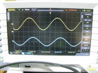
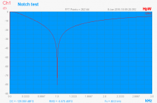
* 3922 shows the other side of the -dB point, 963Hz. So the notch well isn't completely symmetrical at 960Hz, but pretty close.
* In the final photo 3923 I'm trying to get a mesurement on notch depth. The generator is back on 1.0000KHz and I've cranked the scope sensitivity on the output up to 5mV/division. I've turned off the fluorescent room lights to reduce some noise (the board is still sitting here unshielded), hence the dark picture. The output signal appears to be about 1 division, or 5mV peak to peak. The input signal now showing 480mV p-p on the scope, so somewhere around -40dB notch if I've done the math on that correctly.
It would be interesting to see what the board can do with a more modern chip! Lol, at this point I'm going to have to figure out why the LME49990 doesn't work, while the THS4031 does, before trying to pick a different chip.
Continuing from the above post (ran out of photo slots)..
* 3907 and 3908 are 1.0200KHz and 1.0500KHz. I didn't take photos of the other side of the notch at the 20 and 50Hz variation unfortunately.
* 3912 shows the -3dB point, if I did my math on that correctly, and it occured at 1.0400KHz. The scope has the peak of the signal reported below the trace at 264V. I varied the source frequency to set the peak of the output (blue) to 184mV, which is as close as I could get it to 186mV. Unfortunately the scope's measurement kept bouncing back and forth between 184mV and 192mV. Looks like the camera captured the latter.
* 3922 shows the other side of the -dB point, 963Hz. So the notch well isn't completely symmetrical at 960Hz, but pretty close.
* In the final photo 3923 I'm trying to get a mesurement on notch depth. The generator is back on 1.0000KHz and I've cranked the scope sensitivity on the output up to 5mV/division. I've turned off the fluorescent room lights to reduce some noise (the board is still sitting here unshielded), hence the dark picture. The output signal appears to be about 1 division, or 5mV peak to peak. The input signal now showing 480mV p-p on the scope, so somewhere around -40dB notch if I've done the math on that correctly.
It would be interesting to see what the board can do with a more modern chip! Lol, at this point I'm going to have to figure out why the LME49990 doesn't work, while the THS4031 does, before trying to pick a different chip.
Attachments
Last edited:
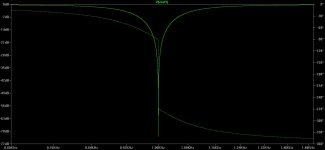
Even better notch with the trimpot!
I ran out of edit time on the post above. I completely forgot about the frequency-adjust trimpot on the board. About 20 degrees of clockwise rotation (I centered that 25-turn pot before solding it in) it appears to have completely zeroed out the 5mV p-p output I was seeing at 1.0000KHz. So apparently the notch is even deeper than -40dB. Going up to 2mV sensitivity on the scope there is so much noise, without being in a shielded box, that I really can't extract anything useful in terms of notch output although it "looks" flat. So at this point I can't say what the actual notch depth is, other than "greater than -40dB"
Time to hook up the QA400.
Speaking of shielded boxes, this board would fit inside the same Hammond 1598REBK case I used for the Victor oscillator board power supply project I have posted in another thread. That case can take a roughly 140 x 140mm board. This one is 130 x 120. I have 3mm mounting holes at the corners of this one that will fit M3 nylon standoffs. I don't have holes in this one to match up with the 4 mounting studs molded in the bottom of that case, so you would have to drill 4 mounting holes up through the bottom of the case.
I ran out of edit time on the post above. I completely forgot about the frequency-adjust trimpot on the board.
About 20 degrees of clockwise rotation (I centered that 25-turn pot before solding it in) it appears to have completely zeroed out the 5mV p-p output I was seeing at 1.0000KHz. So apparently the notch is even deeper than -40dB. Going up to 2mV sensitivity on the scope there is so much noise, without being in a shielded box, that I really can't extract anything useful in terms of notch output although it "looks" flat. So at this point I can't say what the actual notch depth is, other than "greater than -40dB"Time to hook up the QA400.
Speaking of shielded boxes, this board would fit inside the same Hammond 1598REBK case I used for the Victor oscillator board power supply project I have posted in another thread. That case can take a roughly 140 x 140mm board. This one is 130 x 120. I have 3mm mounting holes at the corners of this one that will fit M3 nylon standoffs. I don't have holes in this one to match up with the 4 mounting studs molded in the bottom of that case, so you would have to drill 4 mounting holes up through the bottom of the case.
Attachments
Last edited:
Nice work! Thanks for the details you put into your projects.
Not sure if the QA400 provides a frequency response test. ARTA has frequency response and STEPS to plot frequency response. I used the basic FR test in ARTA to help tune the notch filter I built based off of Dick Moore's design.
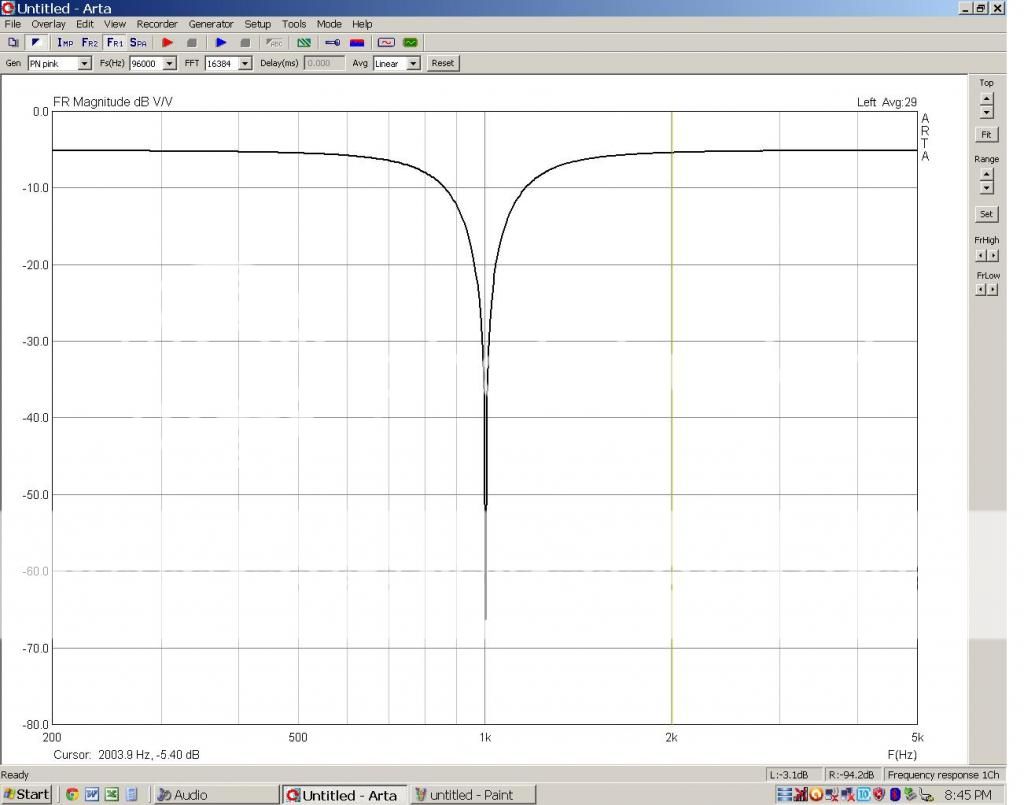
Not sure if the QA400 provides a frequency response test. ARTA has frequency response and STEPS to plot frequency response. I used the basic FR test in ARTA to help tune the notch filter I built based off of Dick Moore's design.

ARTA has frequency response and STEPS to plot frequency response. I used the basic FR test in ARTA to help tune the notch filter I built based off of Dick Moore's design.[/URL]
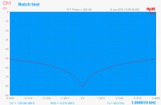
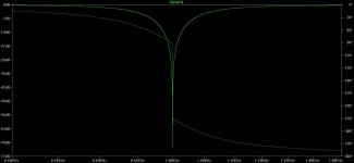
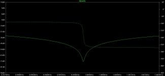
To measure/plot a notch need some special treatment
As currently on my upcoming FFR (Fast Frequency Response) implementation, I have seen some important tasks:
- your notch lowest level should be above the ADC noise floor
- resolutions steps below 1 Hz (even 1/10 Hz) may required, what is notch performance dependent. Currently I do not have any -100 dB or higher notch in my test lab available
- keep an eye of the required notch input impedance
- using steps frequencies would be a time consuming task
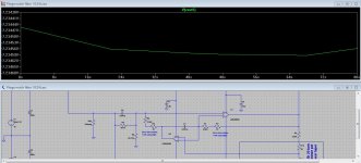
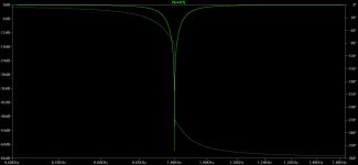
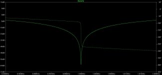
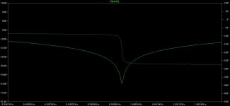
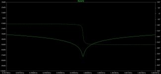
Attached some pictures of my today measured performance..
Hp
Attachments
Last edited:
skidave: thank you for the comments!
I have the ARTA software loaded but never did pick up a good sound card for it. I was in the process of tracking one down (most seem to be discontinued) when I learned about the Q400. I haven't had a chance to do any more measuring but I'll find out what the Q400 can do here.
HpW: good thoughts! In fact I'm going to do some of that. My signal generator will do 1/10 Hz. I've been thinking that I should have tried 0.2 and 0.5Hz given how quickly that signal shot up on either side of the 1KHz with just +/-1Hz
It also hit me that all I need to do improve the S/N for the notch bottom is turn up the input signal generator amplitude! I was only using 500mV p-p. The generator should be able to do at least 5V p-p. Since the whole thing is running on +/-15.3Vdc the chips shouldn't have a problem with 5Vp-p input. The higher input should bump the output up 10x.
I've attached the Gerbers and BOM, below. I have the THS4031 in the BOM now in place of the LME49990. I have the BOM spreadsheet in 3 separate sections: the notch filter parts, the post-amplifier parts, and the AC power supply parts. The filter parts section include the battery terminals and voltage regulator parts.
I'm going to make one other part change. Given that just a tiny 20 degree turn on the 25-turn 50R frequency adjust pot nulled the filter, I'm changing that to 10R. That should give more like a half-turn of adjust range in either direction.
Another issue occured to me about the fairly narrow notch well (higher Q at Q=13): potential temperature drift of either the signal source or the parts in the filter. However I've used fairly low-tempco parts, the 1% NPO/C0G frequency set caps, 25 PPM/C 0.1% frequency set resistors, and the 15PPM/C 0.1% Q set resistors. About the worst tempco part is that trimpot, at 100 PPM/C! Going to 10R should help with that, too, by reducing the adjust range. So long story short if someone finds that the signal is temperature-drifting out of the notch over time a lower Q, like maybe 10, might be in order.
When I measure it again I want to measure insertion loss too. The Fliege is supposed to be 1x voltage gain. I think it is pretty close to 1. Just messing with the signal generator the day I measured it I cranked it up to 1250 HZ or so and beyond briefly. The output and input signal looked to be nearly the same in amplitude on the scope.
I'm going to have one extra board. If anyone is interested it is yours at-cost, plus whatever actual shipping cost turns out to be. Just send me a PM. I paid $130 for 5 boards at PCBway.com, 4 layer 120x130mm HASL, (includes the $25 DHL to get them to me from China), so $130/5 = $26 plus actual shipping cost. I didn't get a bigger quantity because I figured something would be screwed up somewhere. I'm also not planning to take the time to write up build instructions on this one, so you would be on your own a bit in assembling it (although I can certainly answer questions vs PM!). I'm going to build up 3 of the boards for different frequencies for my use and one for test.
I have the ARTA software loaded but never did pick up a good sound card for it. I was in the process of tracking one down (most seem to be discontinued) when I learned about the Q400. I haven't had a chance to do any more measuring but I'll find out what the Q400 can do here.
HpW: good thoughts! In fact I'm going to do some of that. My signal generator will do 1/10 Hz. I've been thinking that I should have tried 0.2 and 0.5Hz given how quickly that signal shot up on either side of the 1KHz with just +/-1Hz
It also hit me that all I need to do improve the S/N for the notch bottom is turn up the input signal generator amplitude! I was only using 500mV p-p. The generator should be able to do at least 5V p-p. Since the whole thing is running on +/-15.3Vdc the chips shouldn't have a problem with 5Vp-p input. The higher input should bump the output up 10x.
I've attached the Gerbers and BOM, below. I have the THS4031 in the BOM now in place of the LME49990. I have the BOM spreadsheet in 3 separate sections: the notch filter parts, the post-amplifier parts, and the AC power supply parts. The filter parts section include the battery terminals and voltage regulator parts.
I'm going to make one other part change. Given that just a tiny 20 degree turn on the 25-turn 50R frequency adjust pot nulled the filter, I'm changing that to 10R. That should give more like a half-turn of adjust range in either direction.
Another issue occured to me about the fairly narrow notch well (higher Q at Q=13): potential temperature drift of either the signal source or the parts in the filter. However I've used fairly low-tempco parts, the 1% NPO/C0G frequency set caps, 25 PPM/C 0.1% frequency set resistors, and the 15PPM/C 0.1% Q set resistors. About the worst tempco part is that trimpot, at 100 PPM/C! Going to 10R should help with that, too, by reducing the adjust range. So long story short if someone finds that the signal is temperature-drifting out of the notch over time a lower Q, like maybe 10, might be in order.
When I measure it again I want to measure insertion loss too. The Fliege is supposed to be 1x voltage gain. I think it is pretty close to 1. Just messing with the signal generator the day I measured it I cranked it up to 1250 HZ or so and beyond briefly. The output and input signal looked to be nearly the same in amplitude on the scope.
I'm going to have one extra board. If anyone is interested it is yours at-cost, plus whatever actual shipping cost turns out to be. Just send me a PM.
I paid $130 for 5 boards at PCBway.com, 4 layer 120x130mm HASL, (includes the $25 DHL to get them to me from China), so $130/5 = $26 plus actual shipping cost. I didn't get a bigger quantity because I figured something would be screwed up somewhere. I'm also not planning to take the time to write up build instructions on this one, so you would be on your own a bit in assembling it (although I can certainly answer questions vs PM!). I'm going to build up 3 of the boards for different frequencies for my use and one for test.Attachments
Last edited:
Q reduced to 5 for deeper notch + DC plot with THS4031
Turns out TI has a Spice model for the THS4031. I've plugged that into LT Spice and checked the DC output now with the new chip. Same behavior as with the LME49990, just with the polarity reversed.
The first transient plot below is with 49.9 ohm to ground on the input again, the THS4031 chips, the Q set resistors now at 33K (see below), and the power supplies at +/-15.3 to match the voltage regulators. The output is 31mV.
Then with the second plot the input resistor is 500 meg to simulate having no input resistor. The DC output now shoots up to +12.5Vdc, same as before but now positive instead of negative voltage. I'm sure the polarity change is just due to chip differences.
Then the rest of the plots are AC plots messing around with the Q and "Q set" resistors R5 and R6 on the Spice schematic.
The first schematic and following 3 AC plots are with the "Q set" resistors at the previous 88.7K for a Q of 13. The notch depth simulates to somewhere around -63dB.
BUT... with the "Q set" resistors changed to 33K in the next schematic and following 3 AC plots, the notch depth is now down to -74dB! Exactly what Rod Elliot said on his Fliege notch filter website page here:
Active Filters
The lower Q results in a deeper notch. The spread is greater, but as Rod says the 2nd harmonic is still significantly reduced.
Given this I'm going to change the standard "Q set" resistors to 33K for a Q of 4.87. I'm picking that number because Mouser just happens to have a 0805-sized thin film resistor in stock with 33K, 0.05% and just 10PPM/C tempco - for only $1! Can't beat that (Mouser part #667-ERA-6ARW333V ). In messing with the simulations the absolute value of the Q set resistors isn't all that important, but having them exactly match each other is for a symmetric notch well.
Attachments
-
 DC output freq=0 Rin=49.9.JPG132.6 KB · Views: 116
 -
 DC output freq=0 Rin=500meg.JPG132.8 KB · Views: 71
 -
 schematic Q=13.jpg163.8 KB · Views: 94
 -
 ac plot Q=13.jpg38.9 KB · Views: 89
 -
 ac plot Q=13 zoom 1.jpg41.8 KB · Views: 70
 -
 ac plot Q=13.jpg zoom 2.jpg40.8 KB · Views: 67
 -
 ac plot Q=4.87 zoom 2.jpg42.2 KB · Views: 67
 -
 ac plot Q=4.87 zoom 1.jpg42.3 KB · Views: 85
 -
 ac plot Q=4.87.jpg41.3 KB · Views: 94
 -
 schematic Q=4.87.jpg163.8 KB · Views: 87
Last edited:
Nice project!
I have some inputs, which I hope can help you with some of the issues you have with the design. And an input regarding noise.
I have worked with the LME49990 as well. A very nice op-amp, but stability can be an issue.
Stability/decoupling:
The data sheet suggests to use three capacitors per rail. In your LTSpice schematic you have used 2.2uF for decoupling. This value may not be the ideal value at 100MHz. I typically use a 100nF X7R capacitor in parallel with a 10uF tantalum. This seems to work well.
In the layout you seem to have large holes in the ground plane. That means that the return path from the positive to the negative supply is rather long, potentially giving an inductance, which is too high. And the magnetic field from the currents flowing around the hole may couple into your circuit.
Is it a problem to have e.g. a 50 ohm resistor in series with the output? It can very often help in terms of stability.
Offset:
The LME49990 seems to use some kind of bias cancellation circuit. Therefore the polarity of the bias current may not be known. The THS4031 on the other hand does not seem to have it, so the polarity will be known, given by the NPN input transistors.
Noise:
If you can live with a lower GBW product the OPA209/OPA2209 might be a better solution. I used it when I made a notch filter a couple of years ago. With the impedances you have in the circuit it will probably give you a much lower noise than LME49990 and THS4031, since the current noise will give a rather large contribution.
JensH - I really appreciate the feedback! Very helpful.
The multi-cap bypass debate is an interesting one! opc made a good post supporting a single capacitor bypass a couple of months ago in his Wire thread (the Wire uses LME49990s) here (post 2419)
http://www.diyaudio.com/forums/head...-headphone-amplifier-pcbs-49.html#post4492334
I've seen triple parallel bypass discussed a lot too. I've more or less decided that the typical 0.01uF and 0.1uF portion of a triple can probably be rolled up into a modern 1uF or just 0.1uF X7R MLCC. I do like the idea of a tantulum bulk cap neaby though! So many of the datasheets have a tantalum bulk cap as one of the three.
So I agree, if I should do a board re-spin one of these days I'll put parallel pads for an optional 10uF or so SMD tantalum. I've also discovered there is such a thing as a 4.7uF 0805 sized X7R MLCC (35V) these days and ordered a bunch, Mouser #810-C2012X7R1V475K1E. I'll probably swap out the 2.2uF's for those.
The oscillation I was getting with the LME49990 chips was *bad* too. 500mV or so peak amplitude of a somewhat distorted sine wave at 3MHz. A little radio transmitter.
Good observation on the ground plane hole. That hole is responsible for 15mm of extra board length on this one. Originally the strip between the batteries and the filter circuit was much thinner. The more I looked at that I wanted a much wider strip there for lower Z. The issue is also another reason I wound up going with pcbway.com again for the fabrication rather than seeed studio. pcbway uses 1oz copper on the internal layers while seeed uses just 1/2oz.
If I do respin the board one of these days I'm thinking that I might make it in the shape of that Hammond 1598REBK shielded case again, with the 4 mounting holes that match the case mounting bosses. That would add around 10mm or so to both the board width and height, increasing the amount of copper around the hole.
On the output resistor, it actually does have a 49.9R in series with the output. I agree, a good idea to help isolate the BNC cable capacitance and provide a matcing resistance value to reduce reflections.
Good observation about the potential input bias cancellation circuit in the LME49990! That hadn't occured to me. I'll bet it does have one, given the low datasheet input bias current numbers. Hmmm..... for that matter maybe a somewhat-faulty bias cancellation circuit in the chip is related to the oscillation. I could just see a circuit like that interacting with the oscillator feedback loop at a certain frequency.
I've never looked at that OPA209/OPA2209 before! It does look like an interesting chip for this. I'll get a couple and try swapping them in as time permits.
Very helpful.The multi-cap bypass debate is an interesting one! opc made a good post supporting a single capacitor bypass a couple of months ago in his Wire thread (the Wire uses LME49990s) here (post 2419)
http://www.diyaudio.com/forums/head...-headphone-amplifier-pcbs-49.html#post4492334
I've seen triple parallel bypass discussed a lot too. I've more or less decided that the typical 0.01uF and 0.1uF portion of a triple can probably be rolled up into a modern 1uF or just 0.1uF X7R MLCC. I do like the idea of a tantulum bulk cap neaby though! So many of the datasheets have a tantalum bulk cap as one of the three.
So I agree, if I should do a board re-spin one of these days I'll put parallel pads for an optional 10uF or so SMD tantalum. I've also discovered there is such a thing as a 4.7uF 0805 sized X7R MLCC (35V) these days and ordered a bunch, Mouser #810-C2012X7R1V475K1E. I'll probably swap out the 2.2uF's for those.
The oscillation I was getting with the LME49990 chips was *bad* too. 500mV or so peak amplitude of a somewhat distorted sine wave at 3MHz. A little radio transmitter.
Good observation on the ground plane hole. That hole is responsible for 15mm of extra board length on this one. Originally the strip between the batteries and the filter circuit was much thinner. The more I looked at that I wanted a much wider strip there for lower Z. The issue is also another reason I wound up going with pcbway.com again for the fabrication rather than seeed studio. pcbway uses 1oz copper on the internal layers while seeed uses just 1/2oz.
If I do respin the board one of these days I'm thinking that I might make it in the shape of that Hammond 1598REBK shielded case again, with the 4 mounting holes that match the case mounting bosses. That would add around 10mm or so to both the board width and height, increasing the amount of copper around the hole.
On the output resistor, it actually does have a 49.9R in series with the output. I agree, a good idea to help isolate the BNC cable capacitance and provide a matcing resistance value to reduce reflections.
Good observation about the potential input bias cancellation circuit in the LME49990! That hadn't occured to me. I'll bet it does have one, given the low datasheet input bias current numbers. Hmmm..... for that matter maybe a somewhat-faulty bias cancellation circuit in the chip is related to the oscillation. I could just see a circuit like that interacting with the oscillator feedback loop at a certain frequency.
I've never looked at that OPA209/OPA2209 before! It does look like an interesting chip for this. I'll get a couple and try swapping them in as time permits.
Last edited:
On the output resistor, it actually does have a 49.9R in series with the output. I agree, a good idea to help isolate the BNC cable capacitance and provide a matching resistance value to reduce reflections.
BTW: on your simulation schema: V3 & R20 should be connected as serial.
While this would give you a real generator... and from there use the input to output measurement.
Than vary with the R20 from 50 Ohms to 2K Ohms to really simulate user behavior (real generators 50/600 Ohms or power amp = 0.xx Ohms or headphone amp impedance)
Consider also on simulation: Add some stray caps, while 7pF to each PCB trace is good value
Hp
HpW - you are right! I like it. The ideal voltage source will have zero impedance itself of course, so might as well put that input 49.9R in series. Done, on the attached Spice schematic. Now I won't have to remove the input voltage source when I bump up that input resistor for DC output offset sims.
Also a good suggestion on the parasitic trace capacitance! I have ground as the second layer on the board, then everything notched out under the feedback loop and inputs. The pp-amp output traces are all above the ground/power planes though. I've taken your suggestion and added 7pf to each. I like adding parasitics to the sim. I have 0.001R on all the MLCC ceramics. I may mess around with adding a few pf of parasitic capacitance *between* the long parallel traces too, on the notched out area. Also might try adding a small amount of series parasitic inductance to those traces.
I've also changed all the 2.2uF bypass caps to 4.7uF since those are in the mail. I'll swap them when they arrive. I do like that suggestion JensH made of more bulk capacitance on the bypass, either larger MLCCs and/or parallel tantalums.
I looked at the OPA209 some more today and may have found a glitch. The TI white paper was saying that a GBW of 100MHz was the minimum for a notch in the 10-100Khz range (I'm also going to build one of these up for 10KHz). Looks like the 209 is just GBW = 18MHz. I did some searching today on the op amp offerings from LT, TI, and AD. Looks like there is actually very little that is over 100MHz AND unity gain stable. Most of the chips over 100 seem to be minimum closed loop gain of 4 to 10. That is a plus for the 209, it does appear to be unity gain stable, from the conditions in the table for the THD specification.
I've also added the 49.9R to the output line in the sim schematic so it matches the board. I've upped the internal series resistance of the 15.3Vdc power rail sources to 0.1R from 0.01R to better model the LT voltage reg chips.
Attachments
Last edited:
- Home
- Design & Build
- Equipment & Tools
- Fliege 1kHz notch filter project PCB