Hi there,
This is a project I had wanted to carry out for a long time: about 10 years ago at my workplace, they decided to get rid of large numbers (100's) of HP428B units.
A good proportion was still in working condition, but I had no way of salvaging them: my available storage space at work or at home was limited, and anyway the company policies forbid any recuperation: they had to be scrapped.
For me it was a heartbreak, because these were nice instruments, well designed, well built, and still usable today even putting aside their historical value.
I did what I could: I kept two units, one at work and one I took back home.
Since the probes were much smaller, I kept a good number of them, thinking that some day I would build a modern conditioning unit for them.
That day has finally come.
I will describe a completely compatible mainframe, offering not only the same functions of the original meter, but also additional ones, with increased accuracy, bandwidth, range, resolution and stability.
Why would anyone bother to do such a thing?
The HP428 was a remarkable instrument, and it remains so 40 years later: this clip-on milliammeter combined DC capability with an exceptional sensitivity: on the most sensitive range, it boasted a whopping 1mA FSD, something that leaves in the dust modern Hall-based meters.
How did the HP guys achieve such a feat?
They used a closed version of a fluxgate magnetometer, the key to the sensitivity and DC capability.
There is more to it than that, of course: to make a good multirange instrument, you need some more ingenuity.
The result was a very nice and convenient meter, even by today's standards.
With hindsight, it has some weaknesses too, but they are only apparent now, and can be fixed relatively easily.
The main problem for me was the bulk: it is typical of 50's-60's equipments, large sheet metal case and heavy.
Another issue was the durability: it was a mainly tube instrument, and some day the question of maintenance will surface.
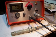
This is how an original HP428 looks like:
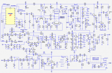
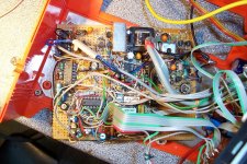
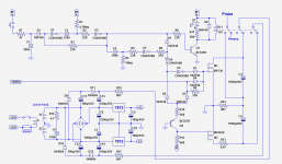
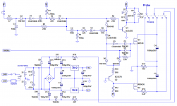
This is the compatible unit I built, and the schematic of the main circuit:
This is a project I had wanted to carry out for a long time: about 10 years ago at my workplace, they decided to get rid of large numbers (100's) of HP428B units.
A good proportion was still in working condition, but I had no way of salvaging them: my available storage space at work or at home was limited, and anyway the company policies forbid any recuperation: they had to be scrapped.
For me it was a heartbreak, because these were nice instruments, well designed, well built, and still usable today even putting aside their historical value.
I did what I could: I kept two units, one at work and one I took back home.
Since the probes were much smaller, I kept a good number of them, thinking that some day I would build a modern conditioning unit for them.
That day has finally come.
I will describe a completely compatible mainframe, offering not only the same functions of the original meter, but also additional ones, with increased accuracy, bandwidth, range, resolution and stability.
Why would anyone bother to do such a thing?
The HP428 was a remarkable instrument, and it remains so 40 years later: this clip-on milliammeter combined DC capability with an exceptional sensitivity: on the most sensitive range, it boasted a whopping 1mA FSD, something that leaves in the dust modern Hall-based meters.
How did the HP guys achieve such a feat?
They used a closed version of a fluxgate magnetometer, the key to the sensitivity and DC capability.
There is more to it than that, of course: to make a good multirange instrument, you need some more ingenuity.
The result was a very nice and convenient meter, even by today's standards.
With hindsight, it has some weaknesses too, but they are only apparent now, and can be fixed relatively easily.
The main problem for me was the bulk: it is typical of 50's-60's equipments, large sheet metal case and heavy.
Another issue was the durability: it was a mainly tube instrument, and some day the question of maintenance will surface.
This is how an original HP428 looks like:
An externally hosted image should be here but it was not working when we last tested it.
An externally hosted image should be here but it was not working when we last tested it.
This is the compatible unit I built, and the schematic of the main circuit:
Attachments
You are to be commended. This is a great project and one I have longed to do myself. I own 40 of the HP428B; perhaps only half on them will live to be restored. Maybe 10 are restored and working at this point. The model 428 design rights were taken on by Applied Physics Systems of Mountain View CA years ago and they make (made?) the 428C and 428D. The APS website is down today and I don't know what that means. I own 3 or 4 of the 428Cs but a new 428D runs around $4000USD and they charge $1000USD for a new probe that is identical to to original HP models. Good work.
Thanks, it is good to see other people sharing interest for this instrument.You are to be commended. This is a great project and one I have longed to do myself. I own 40 of the HP428B; perhaps only half on them will live to be restored. Maybe 10 are restored and working at this point. The model 428 design rights were taken on by Applied Physics Systems of Mountain View CA years ago and they make (made?) the 428C and 428D. The APS website is down today and I don't know what that means. I own 3 or 4 of the 428Cs but a new 428D runs around $4000USD and they charge $1000USD for a new probe that is identical to to original HP models. Good work.
As I said, my main priorities in this project were real estate reduction (my lab is cramped, and 75% of my instruments have to be shelved, some in the attic) and ensuring long term perpetuation, without the fear of lacking some crucial spare part.
Of course, since I started from scratch, I took the opportunity to add functionalities and improve performances.
- The original instrument was essentially DC-oriented: it was actually a clone of an ordinary ammeter, to the point of requiring the correct polarity, although the internal circuitry is completely bipolar.
This output has a bandwidth of 400Hz, which is respectable for a "DC" instrument, but doesn't take you very far with modern electronics.
In the sixties, it was sufficient to examine mains waveform distortions, but today you need more than the eighth harmonic to make serious measurements for even this humble task.
- Thus, the first thing I wanted to improve was the bandwidth, to be able to use it as an AC instrument and oscilloscope interface.
Since I use a frequency divider for the signal generation, taking the next output was easy, and would bring the frequency to 25KHz, safely close to the initial 20KHz.
Of course, the drive transformer also needed to be adapted: I made a dual primary with a quadrifilary winding that could be connected in series or parallel.
In the end, 50KHz proved OK, but as the 2.5x increase alone would only have led me to 1KHz, I figured out that by optimizing the synchronous demodulator, the loop control and the filters, I would be able to reach 5KHz.
- I included AC functions: rms of course, average, rms including DC and even rms calibrated average.
- I used a digital readout, meaning dual polarity without needing to care about the probe polarity, and improved resolution and accuracy.
Of course, this required more than simply using an ADC: the stability and control had to be commensurate.
- I also found the 10 amp maximum current a bit limited: I increased it to 20A, and using the auxiliary output, it can be pushed to 35A before the servo reaches saturation.
I also took the gamble of including a 200µA range.... Did I succeed? More or less, I'll come back on that later.
- Finally, I added another facility: a fully electronic and automatic degausser.
With the integral degausser, you just push the button, and after 1 sec, it's done. You do not even have to remove the probe from the circuit.
The improvement is like night and day, even if there are some limitations.
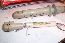
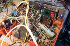
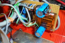
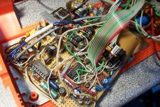
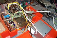
Here is the display board, and some more pics: first, a dismantled probe, and a view of the inside.
On the bottom is the main board, on the left is the supply/degausser
Attachments

Last edited:
Operation:
Master Clock
The master clock is generated by U1. The source is a 6.5MHz crystal, divided by 128 to produce the 50.8KHz of the excitation frequency, which is the filtered and applied to the power amplifier.
This arrangement is perfectly stable, both in amplitude and frequency, thus contributing to the overall stability.
The amplifier itself works in closed loop, for the same reasons.
U1 also provides all the other timing signals: the reference 101.6KHz for the demodulators, the 1600Hz degaussser clock, and a 400Hz clock for the rms/DC converter.
Note that the absolute frequency is unimportant, and other crystals could be used.
Probe Circuits
The drive is applied to the probe via an isolating transformer (the only custom magnetics of the circuit), whilst its output goes to the preamp via the degauss relay.
The zero corrections are also applied there, as DC offset currents.
This differs from the "historic" model, where the correction was achieved by means of a 100KHz of suitable phase and amplitude.
I could simplify that part, because the drive is cleaner and better balanced meaning less out of phase 100KHz components that risked saturating the amplification chain.
The preamp includes a first filter, of very low selectivity and a step attenuator linked to the range switch: this keeps the overall loop gain constant for all ranges, something particularly important for this clone because of the extensions.
A 150KHz notch filter is included, because the probe generates lots of rubbish, a load of odd harmonics. Since the 3rd is close to the 2nd, the rejection of the filters is insufficient to remove it sufficiently.
Finally, a last bandpass filter perfects the frequency response before the synchronous demodulation.
Initially, I had thought I could dispense with it, but there were too many spurious frequencies.
Synchronous Demodulator
Before the demodulation, the signal is converted to balanced and somewhat amplified, then applied to two sections of a 4053 performing the demodulation.
The reference is a properly phased 100KHz derived from the master divider.
The balanced demodulated output is converted back to single-ended and applied to the loop amplifier.
Loop Amplifier
U3B provides most of the loop gain, and as a consequence includes most of the correction and compensation components.
It is a relatively critical part, because we want a frequency response as wide and as clean as possible, and the sampling frequency is dangerously close....
Different tradeoffs are possible, depending on the finality: if the main use is as oscilloscope interface, the time domain response should be as clean as possible, but this will reduce the bandwidth
For level or harmonic measurements, the width and flatness of FR is paramount.
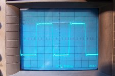
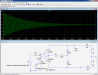
Since I need a bit of both, I adopted an intermediary adjustment: I arrived at almost 10KHz BW (8KHz exactly), but had to tolerate some overshoot and ringing, see oscillogram below of a 450Hz squarewave.
The output of U3B drives the balancing current into the probe, and U3C, D extract the exact value of the current across the shunts.
To be continued...
- I didn't depart fromr the core architecture of the original 428: the probe was designed to be used in a certain way, and reusing the same principles is certainly the shortest path to a working and effective clone, which is my goal here.
I am certain that the probe could be used in a totally different manner, and still give acceptable results, but I didn't want to engage in some creativity exercise, as it would require much more work for an uncertain result (could be fun though).
Master Clock
The master clock is generated by U1. The source is a 6.5MHz crystal, divided by 128 to produce the 50.8KHz of the excitation frequency, which is the filtered and applied to the power amplifier.
This arrangement is perfectly stable, both in amplitude and frequency, thus contributing to the overall stability.
The amplifier itself works in closed loop, for the same reasons.
U1 also provides all the other timing signals: the reference 101.6KHz for the demodulators, the 1600Hz degaussser clock, and a 400Hz clock for the rms/DC converter.
Note that the absolute frequency is unimportant, and other crystals could be used.
Probe Circuits
The drive is applied to the probe via an isolating transformer (the only custom magnetics of the circuit), whilst its output goes to the preamp via the degauss relay.
The zero corrections are also applied there, as DC offset currents.
This differs from the "historic" model, where the correction was achieved by means of a 100KHz of suitable phase and amplitude.
I could simplify that part, because the drive is cleaner and better balanced meaning less out of phase 100KHz components that risked saturating the amplification chain.
The preamp includes a first filter, of very low selectivity and a step attenuator linked to the range switch: this keeps the overall loop gain constant for all ranges, something particularly important for this clone because of the extensions.
A 150KHz notch filter is included, because the probe generates lots of rubbish, a load of odd harmonics. Since the 3rd is close to the 2nd, the rejection of the filters is insufficient to remove it sufficiently.
Finally, a last bandpass filter perfects the frequency response before the synchronous demodulation.
Initially, I had thought I could dispense with it, but there were too many spurious frequencies.
Synchronous Demodulator
Before the demodulation, the signal is converted to balanced and somewhat amplified, then applied to two sections of a 4053 performing the demodulation.
The reference is a properly phased 100KHz derived from the master divider.
The balanced demodulated output is converted back to single-ended and applied to the loop amplifier.
Loop Amplifier
U3B provides most of the loop gain, and as a consequence includes most of the correction and compensation components.
It is a relatively critical part, because we want a frequency response as wide and as clean as possible, and the sampling frequency is dangerously close....
Different tradeoffs are possible, depending on the finality: if the main use is as oscilloscope interface, the time domain response should be as clean as possible, but this will reduce the bandwidth
For level or harmonic measurements, the width and flatness of FR is paramount.
Since I need a bit of both, I adopted an intermediary adjustment: I arrived at almost 10KHz BW (8KHz exactly), but had to tolerate some overshoot and ringing, see oscillogram below of a 450Hz squarewave.
The output of U3B drives the balancing current into the probe, and U3C, D extract the exact value of the current across the shunts.
To be continued...
Attachments
The next block is the Power Amplifier/Shunt Driver:
Nothing special there. Initially, I had adopted a different configuration: the PA was built as a controlled current source, which meant its input voltage was an exact image of the shunt current. I reused exactly the same elements rearranged in a different manner to arrive at this voltage-mode amp, hoping to improve the performances, but basically it didn't change anything significantly.
I had to add the filter L3/C35, to avoid shunting the 100KHz signal from the probe.
With this version, the diff-amp U3D is used to extract the exact shunt voltage.
I didn't change back to the CCS, since its only advantage was in not requiring a filter, and I had already installed the components.
Filters
The signal is then heavily low-pass filtered, first in a somewhat unusual passive circuit: it has a notch at 50KHz, and subsequently in a more conventional 3rd order active circuit.
The 200µA requires additional filtering, I will come back on this later.
Output/conditioning
The filtered signal is sent to the auxiliary output and the various functions conditioners: one is a rather conventional absolute value amplifier, and the other is a non-conventional rms to DC converter.
This converter uses a few standard linear functions, and operates on completely different principles from existing topologies. It is therefore not part of this description, but any other standard, AD536-like circuit is also usable there.
Some points require a bit more explaining:
D2's role in the loop amplifier is as an anti-latchup: I noticed during the tests that sometimes, the circuit locked-up because the negative common voltage range of the opamps was exceeded.
It only happened when the oscilloscope probe slipped, or with similar mishaps, and was easily recoverable by changing the range or cycling the power on-off, but I didn't want to take any risk and I implemented this protection.
The 200µA range was a gamble from my part: I was not sure it was going to be usable, but I tried it anyway, first in the "normal" way, ie increasing the shunt resistance and loop gain, but it wasn't stable: the gain was too high, the filters not selective enough and this resulted in a 25KHz oscillation, probably caused by intermod between the 150KHz residues and the regular 100KHz IF.
I resorted to a simple increase of gain in the post amplifier: U4C, and additional filtering made necessary by the high level of noise: magnetic devices excited at a significant power level tend to be noisy, and this fluxgate probe is no exception.
In the end, this range is actually usable, but with a reduced bandwidth, a significant level of noise, and a very finicky zero: basically, this probe is a sensitive magnetometer operating in a closed, shielded circuit, but it remains sensitive to external fields: for example, it makes a very good compass, and it also detects the movement of a fridge magnet 1 meter away!
This means that once the zero has been set, you mustn't move anything: the probe obviously, but also any ferrous object in the vicinity.
For those interested, I have included a model of the probe and its control loop.
It is not up to date, because it is based on the earlier CCS version, and the compensation components values have been refined on the physical prototype, but it gives a rather faithful image of the real circuit and allows an easy exploration of different scenarios and strategies.
Attachments
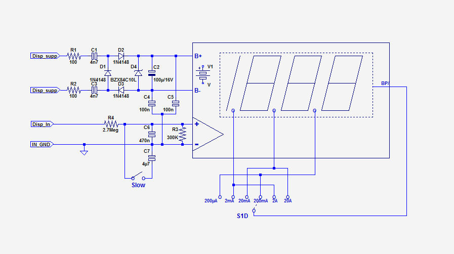
Next function block is the Display Circuit:
Pretty standard stuff for a 7106-based module, except perhaps for the supply: it is derived from the probe exciter.
Since it produces two nice antiphase 50KHz waveforms, it is ideally suited for the job, and the burden of a few more milliamps is completely negligible.
C1 and C3 transmit the power to the floating part of the circuit, and at the same time form an AC divider which results in zero AC voltage on the meter side.
This zero is perfected with the help of C4 and C5.
The signal input undergoes a 10x division: this reduces the offsets of the upstream circuitry by the same factor, making adjustments unnecessary even with standard TLO84 or LF347 opamps. They have just been crudely selected to give a zero reading everywhere.
The time constant of the display filter can be increased by a factor 10, improving the readability on varying currents and particularly on the 200µA range.
The next and final installment will describe the degausser and supply circuit:
Attachments
Last edited:
Supply/degausser:
The core of the supply is completely standard. Things become interesting with the voltage multipliers around D9 to D12: they bring the voltage on R16/17 to ~ +/-45V.
After a sufficient time, C4 and C5 are charged to this level.
When the degauss button is depressed, a one-second one-shot is launched, closing RL1. This disconnects the charging circuit and the probe from the fluxgate, and connects the degausser instead.
After a 100ms delay allowing the relay to settle, the 1600Hz gate opens and the degaussing process begins.
Initially, the peak demagnetization current reaches ~9A (5Ω of the probe/45V), and decays exponentially.
Such a high value may seem widely excessive, but it only lasts a few hundreds µs at a time, and it is required for optimum efficicacy.
Initially, I had tried lower levels, but it wasn't satisfactory.
I had also tried a 800Hz frequency, but the end result was rather random, indicating that the first half-cycle took too long, discharging the caps excessively and magnetizing the probe. In fact, 3200Hz might even be better, but that output doesn't exist on the CD4060.
Anyway, the 1600Hz works fine enough.
Below is an outlook of the current during the demag.
This degausser is very convenient compared to the original instrument's solution, but it has some limitations: even with this high level of current, only the parts very close to the windings can be reached, which means that if the outer µ-metal shell has acquired some remanent field, this degausser won't be able to reach it, because it is too far, yet this parasitic field will be sufficient to skew the zero.
In such a case, a traditional degaussing is the only solution, but it will normally be very rarely needed: in order to create an unrecoverable remanence, I had to touch the probe directly with a neodymium magnet, something that is unlikely to happen under normal circumstances.
Note that there is no need to remove the probe from the circuit during the degaussing, but the circuit should preferably be off: if a significant current circulates during the demag, the zero will tend to align with this current (which is logical after all).
Even with these caveats, this degausser remains a very useful and practical option
Attachments
Elvee,
This is an almost unbelievable accomplishment. A fully "solid-state" 428B. Very commendable!
The 428B has long been one of my favorite HP instruments, along with the 200AB/200CD and a couple of other tube instruments in my collection that I will keep as long as I can keep them running!
Have you given any thought or work on making PCB's for this project? Duplicating what you have done as you know would be a huge task. even for those with the ability to do so.
Seems like a natural task for a SprintLayout6.0 wizard!
All the best,
Sam
W3OHM
Owner and Moderator of the LeCroy_Owners_Group on Yahoo! Groups
ThanksElvee,
This is an almost unbelievable accomplishment. A fully "solid-state" 428B. Very commendable!
Unfortunately no: I don't do PCB's anymore, and anyway for a single unit, it wasn't worth the trouble, revisions, etcHave you given any thought or work on making PCB's for this project?
Questions on L2,3,4 and Q4,5,6 and Shielded part,etc.
Hello Elvee,
Thanks for responding but I have a few more questions:
Do you have more information on the winding of L2,3,4 (core type and source and winding method)?
On Q4/5/6 am I to assume that they are thermally connected in some way?
Also what is in the metal box at the bottom? Is this the TRMS converter? More details?
Also:
Where did you find the dual 47K control and the range switch?
Details on the adjustable and fixed inductors, are all in millihenrys?
A detailed parts list with component types and specs would be handy. Even a simple spreadsheet or handwritten list It is hard to tell from the pictures as to what parts may be critical.
I am wondering if most of this could be done in surface mount maybe on a few interconnected boards for each function as once assembled it should be very reliable.
Do you know if anyone has duplicated your design?
Thanks again,
Sam
W3OHM
Most of the relevant info is on the schematic: core EE20, 3E1 ferrite material, ungapped.Hello Elvee,
Thanks for responding but I have a few more questions:
Do you have more information on the winding of L2,3,4 (core type and source and winding method)?
See p.84 of this document for the modern equivalent:
http://www.ee.bgu.ac.il/~smps/notes/Additional_2012/Ecores.PDF
It doesn't exist anymore in the 3E1 grade, but any of the grades presently available is suitable (and superior to the 3E1).
The wire diameter is 0.23mm (not critical), and the two primaries are bifilarly wound (for convenience mainly, the circuit doesn't really require it).
It is ungapped, resulting in a magnetizing inductance of ~4mH for each of the primaries (IIRC, not critical anyway)
Yes, Q4 thermally compensates Q5 & Q6On Q4/5/6 am I to assume that they are thermally connected in some way?
No, it is the preamplifier part: from Q7 to Q9 approximately.Also what is in the metal box at the bottom? Is this the TRMS converter? More details?
The TRMS is a proprietary circuit I won't disclose, but any AD636-type circuit would do the job equally well
They come from the huge stock I have accumulated over the years. I don't remember their exact originWhere did you find the dual 47K control and the range switch?
No, the unit is indicated: µ=microhenry, m=millihenryDetails on the adjustable and fixed inductors, are all in millihenrys?
Fixed inductors are ordinary, standard chokes.
The variable one is probably for an old TV H-frequency oscillator, I think it came in a Radio Shack grab pack
Very few parts are critical: if you use 1% resistors throughout, that will be sufficient, and of course tuning caps should be a stable type: PP, PS, NPO or PC for example.A detailed parts list with component types and specs would be handy. Even a simple spreadsheet or handwritten list It is hard to tell from the pictures as to what parts may be critical.
The combinations are used to adjust the exact resulting value: for example, C13 and C14 have to create a notch with L6 at exactly 3x the base frequency.
In fact, the main difficulty of the circuits probably resides in the adjustments, rather than the components themselves.
I'll try to provide some details
I think so, however beware of unwanted couplings between the various inductors. If the circuits are too compact, that is a real riskI am wondering if most of this could be done in surface mount maybe on a few interconnected boards for each function as once assembled it should be very reliable.
To my knowledge, noDo you know if anyone has duplicated your design?
Clarification
Thanks again for writing back.
I think I have some ungapped pot type cores that were used for inductors/transformers for stuff in the 20KHz to 100KHz range. Do you think they might work?
One more thing. The there is a transistor pair on the schematic (Q1 and Q1) where the part number is partially obscured. I believe these are BC557B. Is that correct?
Thanks,
Sam
Sam
Thanks again for writing back.
Most of the relevant info is on the schematic: core EE20, 3E1 ferrite material, ungapped.
See p.84 of this document for the modern equivalent:
http://www.ee.bgu.ac.il/~smps/notes/Additional_2012/Ecores.PDF
It doesn't exist anymore in the 3E1 grade, but any of the grades presently available is suitable (and superior to the 3E1).
The wire diameter is 0.23mm (not critical), and the two primaries are bifilarly wound (for convenience mainly, the circuit doesn't really require it).
It is ungapped, resulting in a magnetizing inductance of ~4mH for each of the primaries (IIRC, not critical anyway)
I think I have some ungapped pot type cores that were used for inductors/transformers for stuff in the 20KHz to 100KHz range. Do you think they might work?
One more thing. The there is a transistor pair on the schematic (Q1 and Q1) where the part number is partially obscured. I believe these are BC557B. Is that correct?
Thanks,
Sam
Sam
Yes, in fact most core shapes would work: X cores, RM, etc.Thanks again for writing back.
I think I have some ungapped pot type cores that were used for inductors/transformers for stuff in the 20KHz to 100KHz range. Do you think they might work?
The effective area just needs to be sufficient for the number of turns (which you can alter if required)
CorrectOne more thing. The there is a transistor pair on the schematic (Q1 and Q1) where the part number is partially obscured. I believe these are BC557B. Is that correct?
I am looking at working on some PC boards for this project so I will probably have more questions! Any chance you could post those schematics in the original LTSpice format? I want to plot them out in a larger high res format as I plan to re-enter them in OrCAD schematic format.
On the resistors do you have any that are more than 1/4W.
Sam
On the resistors do you have any that are more than 1/4W.
Sam
Looks like my answer has been ejected....
Bis repetita, etc..
I post the entire (raw) folder, including purely graphic items, working subsections, etc.
Note that all may not be up to date, because final refinements were carried out at a phy level, not in sim.
Bis repetita, etc..
I post the entire (raw) folder, including purely graphic items, working subsections, etc.
Note that all may not be up to date, because final refinements were carried out at a phy level, not in sim.
R65 is a good candidate for a larger size: under normal circumstances, 0.25W is sufficient but in case overloads happen, 0.5W or 1W is preferableOn the resistors do you have any that are more than 1/4W.
Attachments
Hello Elvee,
Thank you for posting that. Now I have to figure out how to use LTSpice .
.
There are at least three Ham friends that I know that are interested in duplicating your fine design. It would be good to know about any circuit refinements before we start working on PCB layouts.
Sam
Thank you for posting that. Now I have to figure out how to use LTSpice
.Looks like my answer has been ejected....
Note that all may not be up to date, because final refinements were carried out at a phy level, not in sim.
There are at least three Ham friends that I know that are interested in duplicating your fine design. It would be good to know about any circuit refinements before we start working on PCB layouts.
Sam
Unfortunately, any of the folders is much larger than 1MB, and even zipped they will be too large for the forum.
Since you're interested in the graphics only, you need practically no models. The only one that you may need is the CD4069, but any inverter will do, and you can rename it on the schematic
Since you're interested in the graphics only, you need practically no models. The only one that you may need is the CD4069, but any inverter will do, and you can rename it on the schematic
- Home
- Design & Build
- Equipment & Tools
- Modernized HP428 clone