Has anyone thought about using switched-capacitor filters at the output of a rectifier?
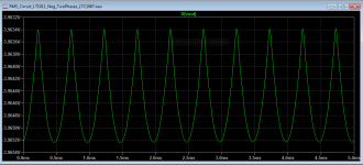
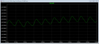
Here are preliminary results of a simulated two-phase, negative peak-value detector with two LT1011 comparators, after the idea of Demian Martin.
First plot shows the output of the comparators filtered by an RC filter with a time constant of 4.7msec, and the second one the output of an LT1067 SC filter with a corner frequency of 1kHz. The remaining ripple appears to have an amplitude of 10uV.
SC filters can track the oscillator frequency, this particular part needs a clock frequency that is 100 times higher than the desired corner frequency, which should not be difficult to generate from the oscillator signal.
Regards,
Braca
Attachments
Why not just use an A-d to measure the oscillator output and then calibrate the cha Ge in signal level during the measurement cycle.
You would have to do this every cycle, but should be quite doable.
Using this approach, you could maybe ditch the AGC and the problems it brings.
You would have to do this every cycle, but should be quite doable.
Using this approach, you could maybe ditch the AGC and the problems it brings.
AFAIK the AGC is a cause of distortion, so they have to be very carefully designed (already discussed here - ripple, usually << Fosc, added distortion etc - see for example JFET AGC with linearizer feedback resistor).
If the osc output is moving around a few percent every few seconds, that should be something that could be calibrated out dynamically and because the output change is only a small % over time, you could probably get away with a 16 bit A-D so you end up with with maybe 20 bits of ripple reduction ref the osc output.
Again, just thinking a loud here.
Really? The SVO's don't have AGC from what I've seen - but I'm open to correction.
As far as I know, every state variable oscillator needs some form of agc control loop. This is not unlike other analog oscillators, like a Wein bridge.
Cheers,
Bob
Has anyone built the 0.5ppm Linear tech Oscillator?
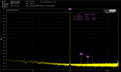
I have built many of these over the years. The lock-down in the US has given me the time to build the 3rd version PCB that is delivering about 10 dB better performance than the 2nd version I've used for a while now. More discussion on the second version is here with some writings on 3rd version here.
The plot below is the current performance of the new REVC board. What you see is the oscillator going into a notch and then that goes into the QA401. Note that the notch correction is swept, saved and then applied in the QA401--what you are seeing is after the signal processing hocus pocus. The THD is about -140 dB and the THD+N is almost -121. The REVC board added a 0..63 dB attenuator (relay-based, with 1 dB steps), 0/12 dB gain on the oscillator and focused a lot on the notch noise. The notch noise is now around -120 dBV (20-20k, no weighting, input referred) and the notch has a fixed 12 dB gain on the output.
The first link above discusses the lineage of the oscillator part of the design. The Jim Williams design from 2011 uses a CdS photocell in the AGC loop, with just a few mV across the CdS resistor (key to distortion). The updated oscillator portion of the design (Januscard) improved on that but also keeps the photocell.
The internal supplies are +/- 15V, so hopefully it will be able to give super clear output from almost +20 to - 63 dBV. The relay code isn't working yet. The last version had some distortions that was dependent on switched attenuator engagement, which I never really understood but thought might be layout related. Hopefully it got a lot better.
If I do another rev, it will include a shield. There is more 1 kHz and 2 kHz leakage in the notch than expected (about -150 dB, which with the 12 dB gain means the leakage is hitting the notch at around -162).
Attachments
As far as I know, every state variable oscillator needs some form of agc control loop. This is not unlike other analog oscillators, like a Wein bridge.
Cheers,
Bob
Clear - thanks
The AGC (or leveling) circuits in most oscillators are responsible for most of the oscillator distortion if very low-distortion operational amplifiers are used. The two main components of the AGC circuit are the rectifier and the gain control device. The latter is often implemented with a JFET (or other voltage controlled resistance – VCR – element). Both of these components create distortion, sometimes one dominating more than the other depending on circuit details. Here I would like to say a few words about the creation of distortion by the rectifier circuit, and ways to mitigate it. The ripple of its filtered output is responsible for distortion by modulating the resistance of the VCR element.
There are other approaches to the required amplitude detection circuit that offer lower ripple than an ordinary rectifier, the most well-known of which is a sample-and-hold circuit. The S-H can provide very good results, but it can be complex, sensitive to timing of the sampling, and dependant on a fairly small sampling aperture. Unless a dual S-H running off of both the positive and negative signal phases is used, whatever ripple it creates is only at 1X the fundamental frequency. All things considered, it can provide very good performance if carefully implemented, but is not necessarily the answer to the maiden’s prayer.
Here I’ll stick with ordinary rectifier types that are simple to implement and are very forgiving in nature. In particular, I’ll show some ripple data from three different rectifier types. These I will refer to as multiphase rectifiers. I refer to a half-wave rectifier as a single-phase rectifier, since it conducts on only 1 phase of the signal and its ripple frequency is 1X the sine wave input frequency. A full-wave rectifier is a 2-phase rectifier.
When implementing an oscillator as a state variable oscillator (SVO), both in-phase and quadrature versions of the signal are readily available. If these two signals are each presented to their own full-wave rectifier (FWR) and the rectifier outputs are summed, a 4-phase rectifier circuit results. Its ripple is very helpfully at 4 times the fundamental frequency, so a given amount of filtering results in much less ripple.
An 8-phase rectifier is implemented in a straightforward way by properly creating versions of the fundamental that are 45 degrees apart. This is easily accomplished with two resistive summing networks that sum equal portions of the fundamental and quadrature signals. Four fundamental signals now result. If these are applied to 4 FWRs, and the results summed (easily by a resistor network of 4 resistors), then an 8-phase (8X) rectifier results. Its ripple frequency is at 8X the fundamental, reducing even further the ripple for a given filter circuit.
There is another matter at work in reducing the ripple as well. The raw unfiltered output of the FWR falls all the way to zero at the signal zero crossings. This creates a lot of ripple to be attenuated by the filter. The raw output of a 4X rectifier does not fall in its valley nearly as far from its peak because the output from the neighboring quadrature-driven FWR comes up to take over while the raw signal is still at a high level (just 45 degrees from its peak point). By the same process, the raw output of the 8X rectifier falls even much less from the peak, creating a raw peak-to-valley voltage that is much smaller. The valley occurs only 22.5 degrees from the peak in time.
A measurement was done in simulation to illustrate the remarkable improvement in ripple when going from 2X to 4X to 8X rectification. A 1 kHz signal of 5-V peak amplitude was applied to the rectifiers. All rectifier outputs were equipped with the same simple first-order R-C filter with a time constant of 3.3 ms. As a baseline, the filtering was chosen so that the 2X rectifier yielded p-p ripple of 100 mV. Gains of all of the rectifiers were normalized to produce the same rectified DC output level of 3.18V.
The raw rectifier output voltages had p-p voltage swings of 5 V, 1.03 V and 0.21 V for the 2X, 4X and 8X rectifiers, respectively. This is an approximate 5:1 reduction in raw ripple for each doubling of rectifier order (14 dB).
Filtered output p-p ripple voltages were 100 mV, 10 mV and 1.2 mV, respectively. This is an approximate 10:1 reduction in filtered ripple for each doubling of rectifier order (20 dB per doubling of order).
These are exceptionally encouraging results for the high-order rectifiers. This performance is especially important for lower-frequency oscillators (like 20 Hz), but still makes a remarkable improvement for a 1 kHz oscillator. The much higher ripple frequency also invites the use of higher-order ripple filters without serious degradation of oscillator agc stability. I’ll show some results in another post.
Some may think the cost and complexity of the 8X rectifier is high. I don’t think so, given what it does for you. Apart from a couple of resistors, it requires 4 full-wave rectifiers. Each FWR requires 2 op amps, 2 diodes and 3 resistors. The rectifier op amps need not be audio-grade. Even a lowly LM324 can do quite well at audio frequencies in a rectifier application. One quad op amp will give you 2 FWRs. Two quad op amps will do the whole job. Op amps, diodes and resistors are cheap these days.
Cheers,
Bob
Hi Bob,
I'm intrigued with your 8 phase rectifier.
I note that when integrator gains are exactly 1 at 1kHz and all resistors are appropriately chosen, there's perfect cancellation of all harmonics below 8th and all remaining harmonics are multiples of the 8th.
Given that, I'm trying to project how much ripple suppression might suffer when voltage-controlled tuning is introduced. To raise the oscillator frequency 1%, the inverter gain must rise 2%, and each integrator's gain will reduce 1%, yielding unity loop gain at 1.01kHz. So now the balance of the 8-phase rectifier is compromised by the 1% difference in integrator amplitudes and there will ripple introduced at 2nd, 4th, 6th, etc harmonics. But I suspect ripple is still low.
Does your simulation project harmonic content in the ripple output?
Thanks.
Best regards,
Steve
These are very good questions, and I have looked into some of them. A great many of the simulations I have done are on a complete SVO with the entire agc loop, so I can look in all of the important places.
A key aspect of the design is that the agc control feedback signal from the first integrator output back to the inverting summer is basically an error injection signal that can be of either phase depending on the operating resistance of the JFET control element. In a perfect condition, this signal is zero. Of course, even when the SVO is perfectly balanced and the fundamental in this signal is zero, there is still the distortion components in this signal. This signal does not usually need to be very large, and it is injected into the inverting summer through a fairly large resistance. What is convenient about this is that one has a signal within the oscillator loop that has distortion that is not that difficult to measure, and it is distortion that is reflective of the much lower distortion in the oscillator output.
These distortion components pass though the forward path of the integrators and are attenuated as expected as they make their way to the oscillator output. This is the main origin of the oscillator's distortion if the SVO op amps are ideal. The agc control circuit I described above is essentially the same as the one I used in the oscillator in the THD analyzer I did back around 1980. The schematic of that can be found on my web page.
Anyway, I usually look at the FFT of this signal, the oscillator output signal, and the signal driving the gate of the agc element.
The signal at the output of the rectifier circuit is quite sinusoidal and at the 8th harmonic. However, this does not mean that it has no effect on lower harmonics of the oscillator output. This can be a bit non-intuitive, but the reason is that the JFET has some nonlinearity. That 8 kHz ripple is being applied to the gate of a JFET, so there is mixing and down conversion that can occur. I have done many simulations to verify this and related behavior, with different amplitudes of ripple and different orders of rectifiers. Anyway, this 8 kHz ripple still must be held small, as it plays a role in creating a good portion of the 3rd harmonic in the output of the oscillator. The key thing to bear in mind here is that the 8 kHz ripple is not being injected into the oscillator signal path, but rather is modulating the gain in the agc control element. indeed, this is the essence of the nonlinearity. In this regard, things would be no different if the JFET was replaced by an ideal multiplier.
The 8X rectifier is very forgiving, but it is certainly true that if the quadrature input to it is of a different amplitude than the in-phase input, some additional harmonics below the 8th harmonic will begin to appear in the ripple. These will usually tend to be at the 4th harmonic in the ripple. I have not done extensive testing on the end effect of slight mismatches in amplitude between the quadrature and in-phase oscillator signals delivered to the rectifiers. Your point is well-taken when we make the oscillator into a narrow-band VCO by slightly altering the main SVO feedback resistance. Indeed, I have created such a VCO using the oscillator I have been simulating, and results are very encouraging in regard to any degradation of the oscillator THD as the frequency is moved by 1% or so in either direction. In a later post I'll present some of those results.
In that same matter, I have done numerous experiments with injection locking of the oscillators, and have had some very interesting results that I will put in another post.
Cheers,
Bob
Slightly OT/: I have started a new thread about distortion in filters due to the capacitive load on some opamps:
https://www.diyaudio.com/forums/equ...itive-load-impact-distortion.html#post6150336
Would appreciate if some of the cognoscenti here would comment.
/OT
Jan
https://www.diyaudio.com/forums/equ...itive-load-impact-distortion.html#post6150336
Would appreciate if some of the cognoscenti here would comment.
/OT
Jan
No, sampling one time per whole period of sine wave is wrong idea. Same apply to peak detectors. The issue is SNR of the AGC loop control. To make signal-to-noise ratio be adequate, averaging over multiple cycles required. Basically, averaging or low passing is the only way. OTOH AGC should have fast response, to stabilize amplitude in a reasonable time frame. To satisfy both conditions, sampling has to be continuous, as fast as possible. Micro CPU calculates RMS each cycle with high level of accuracy, so 16-bits or more and low noise ADC required.I implemented a 4 phase rectifier with LM339's (open collector) as active perfect diodes some time ago. The other virtue of this is that you can get an H2 and H4 signal that can be added back to null out harmonics. This is a trick borrowed from the Amber 3501 oscillator.
Still I think David's trick using an ADC to sample and a multiplying DAC as a gain control is really elegant and simple. Using a fast comparator to sense the zero crossing to trigger the ADC to sample the peak of the cosine is not too difficult to implement. The issue with any of these is to keep any switching transients from getting back into the output. Possibly several isolated supplies would be needed once you are getting below -120 dB since it would not take much crosstalk to show in the output. That is the limitation of the older KH oscillators.
Alternative in the analog domain is an integrator. It's "sampling" all the time right after full wave rectifier, does averaging and LPF filtering.
Attachments
The sample and hold solution has been used effectively to get really stable and accurate AC sources for 50 years. You need to sample at precisely the peak of the waveform but that's the zero crossing of the cosine so not a difficult problem.
The implementation in the Boonton uses a single set of time constants for 10 Hz to 140 KHz with essentially no variation in output to 5 decimals. It also settles really quickly. it does use a number of parts, some of which are types no longer used. That where an ADC can do it very nicely as David proved. Below:
The implementation in the Boonton uses a single set of time constants for 10 Hz to 140 KHz with essentially no variation in output to 5 decimals. It also settles really quickly. it does use a number of parts, some of which are types no longer used. That where an ADC can do it very nicely as David proved. Below:
Attachments
No, sampling one time per whole period of sine wave is wrong idea. Same apply to peak detectors. The issue is SNR of the AGC loop control. To make signal-to-noise ratio be adequate, averaging over multiple cycles required. Basically, averaging or low passing is the only way. OTOH AGC should have fast response, to stabilize amplitude in a reasonable time frame. To satisfy both conditions, sampling has to be continuous, as fast as possible. Micro CPU calculates RMS each cycle with high level of accuracy, so 16-bits or more and low noise ADC required.
Alternative in the analog domain is an integrator. It's "sampling" all the time right after full wave rectifier, does averaging and LPF filtering.
It is true that sampling multiple times during a period is helpful. The 4X and 8X rectifiers I described above do just that in the analog domain. One will always need some form of filtering after the rectifier, and more sampling per cycle reduces the amount of filtering needed for a given amount of rectifier ripple, both because the ripple frequency is higher and because the raw amplitude of the ripple to be filtered is smaller. In addition to the filtering of the ripple, some form of integrator is also almost always used to obtain precision and stability in the oscillator's output amplitude.
Oscillator agc feedback stability and settling time depend a lot on the filtering and integration loop, and a faster loop, made possible by multiphase rectification, can help a great deal. It also depends on the oscillator frequency compared to the time constants in the ripple filter. Using different time constants for each decade of frequency can greatly improve this tradeoff. The biggest challenge in this tradeoff is often the performance at the lowest frequency for the oscillator.
Cheers,
Bob
I've written up my experience in bringing up a Jim Williams/Januscard oscillator paired with a passive notch. I think Demian and Bob's explorations are important as the 2H considerations Williams explained in his article related to LED bias are real. If I build another version, it will be with each block individually shielded to see if it helps. I think the performance limitation at this point is either radiated or conducted 2 kHz from the rectifier into the notch.
Link is here: Notch Filter Hardware REVC - QA401 - QuantAsylum Forum
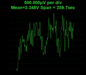
If anyone is curious, the picture I attached is the loop control voltage on the NSL32 LED. This measurement has nV capability, but 400 mS interval, so there could be a lot more action that isn't shown, but given the loop response (~3 sec) probably not.
Each 500uV division corresponds to about 1uA of LED current. So, the loop is making adjustments as small as hundreds of nA to the LED current.
Link is here: Notch Filter Hardware REVC - QA401 - QuantAsylum Forum
If anyone is curious, the picture I attached is the loop control voltage on the NSL32 LED. This measurement has nV capability, but 400 mS interval, so there could be a lot more action that isn't shown, but given the loop response (~3 sec) probably not.
Each 500uV division corresponds to about 1uA of LED current. So, the loop is making adjustments as small as hundreds of nA to the LED current.
Attachments
- Home
- Design & Build
- Equipment & Tools
- Low-distortion Audio-range Oscillator