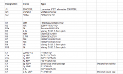
Here is a BoM that the others have been using for their build.
So as far as I know accurate and up to date.
Patrick
The Vishay resistors (R3,R10) -- CMF50 is 3.81mm
For a 1R in 3.81mm pitch, however, a bit difficult to find, perhaps BC Components or Yaego metal film, or a 1610 surface mount device.
This is not the supplier we use, but at least it seems available.
1x S102K 1R0000 1% Vishay S102 Series Metal Foil Resistors Y00621R00000BR0L | eBay
But yes, anything low noise would do, e.g. Beyschlag MELF (Mouser 594-MMA02040C1008FB3).
P.
1x S102K 1R0000 1% Vishay S102 Series Metal Foil Resistors Y00621R00000BR0L | eBay
But yes, anything low noise would do, e.g. Beyschlag MELF (Mouser 594-MMA02040C1008FB3).
P.
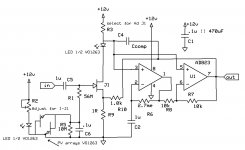
Building the Wurcer LNA
Been looking through the Wurcer LNA courtesy of Xen. Ordered some parts, but more to go.
Question 1.)
The PV array is shown in the sch with the outputs in parallel but in opposite directions. This is replicated in the PCB.
If I set the 10kVR LED current into the PV Array and assume this is fixed.
When the input jFET draws current, it turns on the other LED and generates an opposite output, thus reducing the net voltage/current fed to the input offset injection via the 56Meg resistor.
If the jFET draws more current, the offset current injection is reduced.
Am I interpreting this correctly?
Q2.)
The R2a value is shown as 3k ±0.5%.
This resistor is in series with the 10k Variable R2.
Why is a 0.5% tolerance resistor specified?
Q3.)
The 1k R10 2k5 R3 and the 1r R9 are specified as Vishay S102.
What do these resistors do, that needs this quite specific resistor?
Can any 1r and 1k metal film be substituted?
If not any, what parameters are important for selecting these resistors?
Q4.)
C4 is optional and a 5pF is suggested. A position is not shown on the PCB. Where should this be located?
Attachments
Last edited:
It might be preferable to think about the photovoltaic circuit as a voltage generator. It creates a negative bias voltage "Vgg" that appears across C6. R1 conveys this bias voltage to the gate of the JFET. Meanwhile the JFET's source is very nearly ground; it's (1R * Ids) which is only a dozen millivolts above ground. So the JFET's gate-to-source voltage is (epsilon - |Vgg|). Presto, the photovoltaic circuit sets Vgs which sets drain current.
Yes R2 has a note saying:It might be preferable to think about the photovoltaic circuit as a voltage generator. It creates a negative bias voltage "Vgg" that appears across C6. R1 conveys this bias voltage to the gate of the JFET. Meanwhile the JFET's source is very nearly ground; it's (1R * Ids) which is only a dozen millivolts above ground. So the JFET's gate-to-source voltage is (epsilon - |Vgg|). Presto, the photovoltaic circuit sets Vgs which sets drain current.
Adjust for I - J1
So that fits with what we both said.
But what about the reversed (the other half of the PV array) voltage generator. The control LED comes from the CURRENT into J1.
Q1 to be anwered by the designer of the circuit.
Q2 0.5% is standard tolerance for 0805 Susumu.
Q3 we want to use the best available, so S102. Have not done any analysis. Feel free to use whatever you ee fit.
Q4 Not required in multiple examples built by us. Ele solder directly on the pin of the IC.
Patrick
Q2 0.5% is standard tolerance for 0805 Susumu.
Q3 we want to use the best available, so S102. Have not done any analysis. Feel free to use whatever you ee fit.
Q4 Not required in multiple examples built by us. Ele solder directly on the pin of the IC.
Patrick
Any left?
I am interested if there is a new batch.
SGK - 1
Lbud4 - 1
luvdunhill - 1
")
Q1 to be anwered by the designer of the circuit.
Patrick
I think the basic operation has been covered. The PV acts like a differential current in current out. If you look at the data sheet graphs the gain is about 1uA per mA in the LED for each side so into 10M it's about 10V/mA at the FET gate. The FET runs at only -.5V or so Vgs so you adjust the pot to about the same current as you want Id since there is a lot of gain in the bias stabilizing loop. With 10V/mA and 20mS gm in the FET the optical loop gain is ~200 more than enough to hold the bias stable.
SGK - 1
Lbud4 - 1
luvdunhill - 1
waltzingbear - 2
DNi - 1
- Home
- Design & Build
- Equipment & Tools
- My version of the G = 1000 low noise measurement amp (for Ikoflexer)