Just to correct a POSSIBLE typo in this excellent post
In noise calculations of page 1 post #1 where it says:
"For example, an ideal 1k resistor will (by equation 3) have a noise voltage from 20Hz-20kHz of 5.7nV"
maybe it should read:
"For example, an ideal 1k resistor will (by equation 3) have a noise voltage from 20Hz-20kHz of 569nV"
In noise calculations of page 1 post #1 where it says:
"For example, an ideal 1k resistor will (by equation 3) have a noise voltage from 20Hz-20kHz of 5.7nV"
maybe it should read:
"For example, an ideal 1k resistor will (by equation 3) have a noise voltage from 20Hz-20kHz of 569nV"
Just to correct a POSSIBLE typo in this excellent post
In noise calculations of page 1 post #1 where it says:
"For example, an ideal 1k resistor will (by equation 3) have a noise voltage from 20Hz-20kHz of 5.7nV"
maybe it should read:
"For example, an ideal 1k resistor will (by equation 3) have a noise voltage from 20Hz-20kHz of 569nV"
SY was having a bad period
For those asking, here's the thread on passive equalization for IEC: Passive IEC equalization for tape playback --
Exceptional design and beautiful read !
This is one of the best projects on diyaudio.
Thank you Stuart !
Now that I'm isolated at home with family, have started to learn KiCad. I'm surprised to see that KiCad, in the last years, have evolved a lot and become a powerful tool.
So, here is my 4 days work on SY gorgeous design. Not finished, but wanted to share what I have done so far as open source, so anyone may modify and get his boards at a factory. HMN.zip have all needed files.
Hope is OK.
Regards,
Tibi
Attachments
Last edited by a moderator:
So, here is my 4 days work on SY gorgeous design. Not finished, but wanted to share what I have done so far as open source, so anyone may modify and get his boards at a factory. HMN.zip have all needed files.
Hope is OK.
Regards,
Tibi
You might want to consider that the top DMOS transistor should get some heat sinking as it is doing most of the work. Your design should provide for this.
Thanks !
Which is power dissipated by over top DMOS transistor ?
Regards,
Tibi
Ok, I did some calculations. At 20mA Q2 will dissipate near 2W.
At 10mA Q4 wil dissipate something under 0,6W and Q5 under 1W.
Even at 2W TO220 capsule will be well inside SOA, a small Al heatsink will keep things at safe side.
Other depletion mosfets will run cold.
Regards,
Tibi
This is a simple question:
On the raw supply heater schematic, does the center tap of the secondary 18-20v transformer tie to the middle of the pair of smoothing caps (c129 & c20)? Its goes to pin 2 of the connector, seems like it should but there is no dot where they cross.
anystereo
On the raw supply heater schematic, does the center tap of the secondary 18-20v transformer tie to the middle of the pair of smoothing caps (c129 & c20)? Its goes to pin 2 of the connector, seems like it should but there is no dot where they cross.
anystereo
This is a simple question:
On the raw supply heater schematic, does the center tap of the secondary 18-20v transformer tie to the middle of the pair of smoothing caps (c129 & c20)? Its goes to pin 2 of the connector, seems like it should but there is no dot where they cross.
anystereo
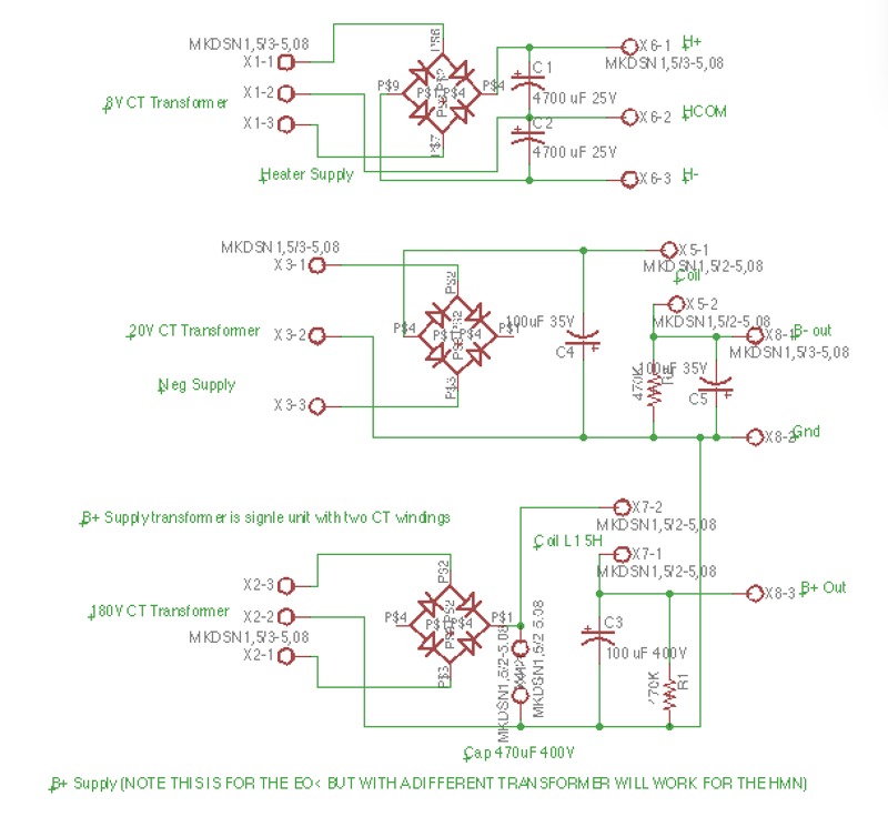
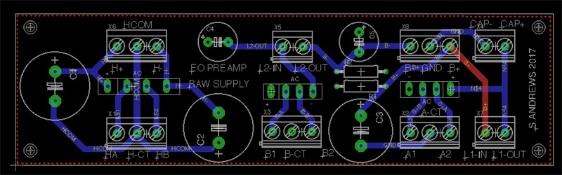
Yes. BUT, because the regulator circuit raises the common point by about 30 +volts, it is NOT grounded!! Here is how I laid it out on the raw supply board. The terminals go off to the big caps and coils that are not on the board.
Note this is for the EO preamp (Moving magnet). Similar design by SY that uses the same supply architecture. IIRC, the heater voltage is different on the HMN, and the B+ supply is much higher, so you will need different transformers.
Last edited:
You might want to consider that the top DMOS transistor should get some heat sinking as it is doing most of the work. Your design should provide for this.
While looking at DN2540 datasheet I see that these devices have positive temperature coefficient, "this device is free from thermal runaway and thermally-induced secondary breakdown".
This also mean that CCS will be temperature dependent and with a heatsink the transistor will need a longer time to settle at operating point.
Considering that TO220 temperature resistance is 29C/W, running at ambient 23C and 2W total power dissipated, the upper transistors in CCS will run hot at max 81C.
With all these considerations, I do not see mandatory the need of large pcb mounted heatsink. A small and light Aluminium heatsink mounted directly on the back of transistor will be sufficient even in a closed enclosure. On the other hand, I see SY running these without heatsink as well. Sometimes runing hot is not a bad thing.
Regards,
Tibi
Last edited by a moderator:
Tibi,
I built the EO MM pre, but SY used essentially the same CCS design. I agree with you that a small, transistor mounted heatsink does just fine. In fact, I'm using a small section of 19mm angle aluminum as a home made heatsink. Since you are doing your own board, just make sure you leave room for the typical U shaped heatsink and you should be good.
Jac
Tibi,
I built the EO MM pre, but SY used essentially the same CCS design. I agree with you that a small, transistor mounted heatsink does just fine. In fact, I'm using a small section of 19mm angle aluminum as a home made heatsink. Since you are doing your own board, just make sure you leave room for the typical U shaped heatsink and you should be good.
Jac
I have not found that the MOSFETS run particularly hot. Warm, but not hot.
I have had nothing but trouble getting the heaters to work properly though.
The EO heaters are lower voltage than the HMN, and it took me a couple of tries to get the transformer output right (didn't help that I was going by the RMS transformer value and not the peak!). On my first cut at those, the 317/337 regs were getting so hot they would go into thermal shutdown after about 5 mins. I could run one board at a time, but they still got pretty hot.
The new design uses an 8V CT transformer (12 Peak). I also run two parallel regs, one for each channel. This seems to work, although the regs still run slightly warm (80 deg C). I found a small u-shaped heatsink did the trick. With that they stabilize at about 40 deg C.
My heater voltage under load is now slightly low (5.6 volts), so I plan to adjust the regulator resistors to get it to 6.3.
Here is my reg board.
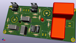
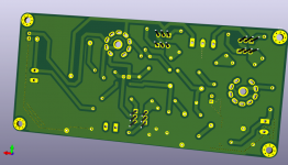
This is final KiCad version. All needed files included as a full open-source project.
Clearance was increased to 1,5mm
Removed some duplicated ground traces and optimised both GND planes.
All parts are marked on PCB with indication which should be MTL - metal for low noise.
RIAA parts also marked on PCB.
Gerber.zip file is ready for production. You may upload at PCB Prototype & PCB Fabrication Manufacturer - JLCPCB and see how will be final look.
You need to order at leat two, one per channel.
Power supply will come later.
Regards,
Tibi
Attachments
- Home
- General Interest
- diyAudio.com Articles
- His Master's Noise: A Thoroughly Modern Tube Phono Preamp