Introduction
In Burning Amp 1 we examined an amplifier circuit designed to complement the hardware we gave away to some attendees at last October's Burning Amp Festival in the San Francisco bay area. This first design centered on a power output stage having of four banks of parallel N channel Mosfets. It was a single-ended Class A amplifier which delivered high quality sound with only local feedback.
Burning Amp 2 will use virtually the same front end and power supply but coupled to complementary banks of N and P channel power Mosfets used as followers in a push-pull Class A configuration.
There is an advantage to the push-pull Class A output stage over the single-ended output stage of the BA-1 as it can be operated more efficiently and delivers much higher output current into load impedances below 8 ohms.
Concept
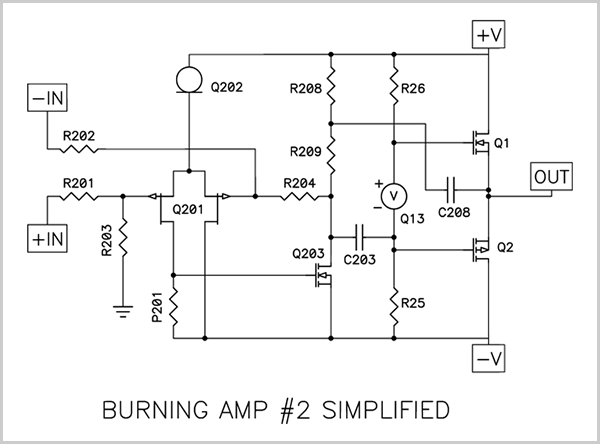
As with BA-1, this amplifier has a voltage gain stage which uses matched P channel Jfets to differentially accept a balanced or single-ended input signal. Following the Jfets, an N channel Mosfet provides single-ended voltage amplification controlled by a local loop. The output stage is a push-pull Class A power follower, biased by a TL431 monolithic shunt voltage regulator.
The component numbers here will correspond to those in later, more detailed schematics. We see the JFET input differential pair Q201 biased by current source Q202, the voltage gain transistor Q203, the output bias voltage source Q13 and the output power followers Q1 and Q2. Local feedback for the front end comes through R204. R201 equals R202, R203 equals R204 and the gain of the balanced front end is set by the ratio of R204 / R202. P201 is a variable resistor which adjusts the DC offset of the front end, and Q203 drives a bootstrapped source formed by R208, R209, and C208.
Power Supply
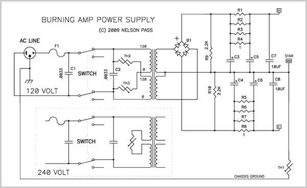
Here is the basic schematic of the power supply. This is essentially identical to many of the power supplies found in earlier articles such as the Zen series and the First Watt amplifiers. The components are fairly ordinary. As the typical Burning Amp will dissipate maybe 300 watts, the transformer wants to be rated at least twice that. The diode bridge is 35 amps at 200+ volts, and you can use ordinary or fancy high-speed bridges as you please. There were a variety of transformers given away with these chassis, and our goal is to have approximately +/- 25 volts on the supply rails. Voltages from 18 to 30 volts are acceptable, and for transformers with secondaries much higher than 20 volts AC, operation using the primary taps in series as shown may reduce the secondary voltages to the desired levels.
C1 and C2 are line-rated types only, as they will be filtering AC line voltages. Thermistors TH1 through TH3 are high power types such as Keystone CL60. TH1 and TH2 are used to suppress inrush surges on turn-on, and also are useful at reducing mechanical noise in the transformers in conditions of high line noise. You will see that the chassis of the amp is to be directly attached to the AC Earth, and TH3 is used to attach analog ground to the chassis through the resistance of TH3, reducing issues with ground loops.
C3 through C6 are your standard high capacity power supply capacitors. The “long” Burning Amp chassis with parallel output devices “6 deep” accommodates four such capacitors, the “shorter” chassis holds two. I recommend that the owners of the “short” chassis to find a way to mount two more capacitors at the front of the amp for C3 and C4. You will also note 10 uF film capacitors across the supply lines. You can delete these, remembering that the prototype used them.
All the resistors in the supply are 3 watt or higher types, and you can see R1 through R8 used to form an RC filter to reduce the supply ripple on the second set of capacitors.
From a layout standpoint, you can wire the supply just as you see on the schematic. The two crucial things to remember is that the ground point labeled STAR is the one you want to bring the signal grounds back to. The other issue is to keep the signal wiring at some physical distance from the transformer, AC lines, and the rectifier bridge and the wires attached to it.
Output Stage
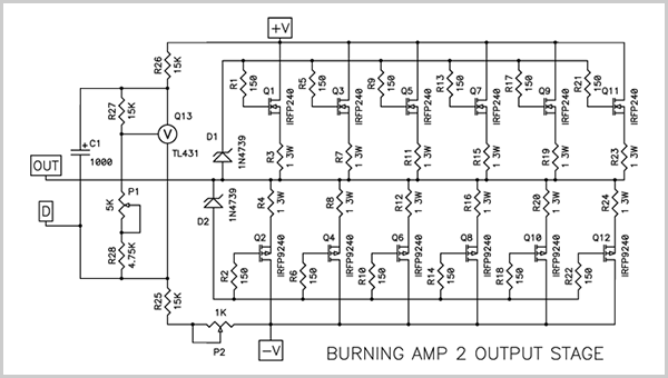
Because this output stage is intended for more than one project, a modular approach is being taken, and we will consider the output stage by itself. Here is the schematic of the “6 deep” output stage. The “4 deep” output stage is achieved by deleting two pairs of output devices and the associated resistors. All the parts are also numbered between 101 and 199.
The 1 ohm resistors are all 3 watt types, and the output devices are best matched for (the) Vgs within about 0.1 volts or so at 500 mA or so. It is not necessary or practical to match the N channel parts to the P channel parts. P101 is used to set the bias current of the output stage, and P102 is used to adjust the output DC offset.
Meet the New Front End. (Same as the Old Front End)
As with the output stage, the front end needs good stand-alone qualities. Besides accommodating single-ended and balanced inputs, we want a range of potential voltage gain figures, the ability to swing the output stage close to the rails, and performance that will not significantly degrade the stand-alone performance of the output stage. Most amplifiers enclose the output stage in the feedback loop with the front end, but that will not be the case here. This is largely the same as BA-1 with the removal of all the output stage biasing elements:
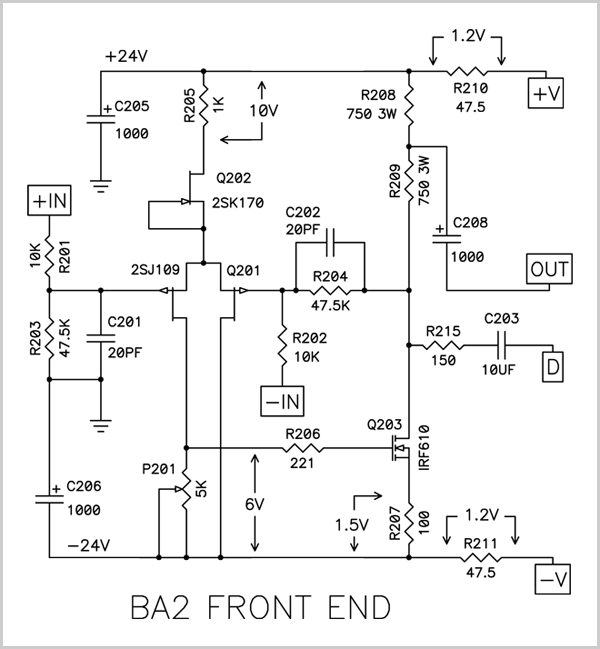
All the parts are numbered in the range of 201 to 299. This front end circuit is different from BA-1 in that it does not include the parts to bias the output stage – those have been shifted to the output stage schematic to make these projects more modular in the future. It also deletes C204, the capacitor from the output of the front end to ground, as it happens that the output stage of BA-2 has more input capacitance than that of BA-1, providing a more optimal amount for a clean square wave response. I have also lowered the gain, although you can put it back in if you like.
Q201 is a dual matched pair of P channel Jfets, part 2SJ109. These are in scarce supply (although the recipients of Burning Amps will each get a pair). They can be substituted with matched 2SJ74 types, and a number of other parts will function with lesser performance.
Q201 is biased by a constant current source formed by Q202 and R205. Q202, an N channel JFET 2SK170 with Idss of about 10 mA, is operated as a constant current source by simply attaching the Gate pin to the Source pin. If you don't have a 2SK170 with the 10 mA Idss, you can parallel two lesser Idss parts. The 10 mA figure is not critical, and potentiometer P201 provides flexibility on the value. R205 takes up some of the dissipation that would otherwise be found in Q202, keeping it within dissipation spec. As shown on the schematic, you will typically see about 10 volts across this part, reflecting the 10 mA current.
R201 through 204 form the balanced inputs networks. R201 = R202 and R203 = R204, and the gain is R204/R202. Compensation capacitors C201 and C202 form the high frequency roll-off for the gain, and while C201 is not strictly essential, it helps to retain the balanced input common mode rejection figure at high frequencies.
When operating the amplifier with a single-ended (RCA) input, the negative input is shorted to ground. You can use dual input connectors, RCA and XLR with the hot RCA connected to pin 2 (+) of the XLR and RCA ground to pin 1. Pin 3 is the (-) input, and can be shorted to pin 1 on the XLR for single-ended input.
The output signal from the input JFET appears across P201 and drives the Gate of Mosfet Q203 which provides the remainder of the voltage gain for the front end. P201 provides adjustment against the expected variations of components in the front end and is used to set the output DC figure of the front end only. No “lag” frequency compensation is employed.
The Drain of the Mosfet Q203 is biased with about 15 mA of current provided by the series 3 watt resistor values of R208 and R209. On the Source of Q203 the gain is degenerated by R207 at 100 ohms, limiting the gain and improving the linearity and bandwidth of this stage.
The point between R208 and R209 is “bootstrapped” from the output of the amplifier through C208. In many designs a constant current source would be employed here, but this approach is simpler.
You will note that RC networks appear between the output node of the front end and the input of the output stage. C203 rolls off the low frequency response at about 2 Hz and I chose to use a 10 uF polypropylene type here, as the only capacitor in the signal path. You could consider using an Elna 10 F silk electrolytic here, in which case you want to orient the + polarity pointed to the left, toward the R215.
R210, R211, C205 and C206 form a supply decoupling filter which helps keep the noise low by filtering the ripple from the raw power supply rails.
Construction Notes
All the usual comments about construction apply to this amplifier. The parallel output devices should be matched for Vgs so that they share current well, and of course we note that all Mosfets are static sensitive until installed in the circuit, so they should be handled with reasonable care. Once in the circuit they are protected by D101 and D102.
Heat sinking for this amplifier is vital, and should be enough that the metal on which the transistors are mounted is at 65 deg C or less, and the fins should be at 55 deg C or less. If they are higher, you need to consider ventilation, fans, and/or lower bias current. The diode bridge for the power supply should also be mounted on metal for heat sinking, and Q203 is best provided with some sort of “push-on-tab” heat sink.
The power transformer should be rated at 600 VA or more. Two channels of this amp will may draw as much as 300 watts, and we allow at least a 2 to 1 transformer margin.
Safety first: Use the smallest value Slow-Blow type fuse that holds up under continuous operation. Start with a 3A value and increase to 4 or 5A if necessary.
More Safety first: The chassis must be solidly grounded to the AC earth ground and should be attached to the analog circuit ground either directly, or through power thermistors or diode bridges if it is necessary to prevent ground loop noise issues.
Initial Turn-on and Adjustments
When the amplifier is first fired up, it is best done without a load. At a minimum you will need a DC multimeter so as to separately adjust the DC offset figures of the front end and the output stage.
The most important things to do before applying power to the circuit are to set the potentiometers to “safe” settings. This means that P201 and P102 should be set at their “middle” positions, and that P101 should be set for maximum resistance. You can use a multimeter to confirm that P101 is at maximum – at one extreme you will measure 0 ohms or so across the potentiometer, and at the other extreme several K ohms. Set it at the maximum resistance extreme.
It is very useful to apply power using a Variac ™ to raise the AC power voltage while checking the current draw of the circuit. It is important to monitor the voltage across the 1 ohm Source resistors of the output devices for current, and also to check across R210 and R211 for excessive voltage. It's best to initially do this with one channel connected to the power supply at a time, and it's also best to do this at low AC power voltages, rechecking at increased voltage.
When you get to the point where full power is applied and there is low current draw by the output stage, that is a good sign. Set P201 to adjust the Drain voltage of Q203 to approximately 0 volts. This value is not critical, as it is isolated from the output in any case.
Then you want to adjust the DC output of the amplifier using P102, again setting it to about 0 volts. You will be adjusting it again later, after you bias the output stage.
Use multimeter to confirm the various voltages which are shown in the schematics to confirm that they are nominally close to those values. You will want to keep an eye on the amplifier as it warms up, and you will end up re-adjusting the values of the potentiometers.
The amplifier prototype I built biased the output stage at 250 mA per output device, which measures as 250 mV across each of the 1 ohm Source resistors on the output stage. You will want to gently adjust P101 to this figure while watching the voltage across one of the 1 ohm resistors. When you reach that figure, use the multimeter to confirm a close value across all the 1 ohm output stage resistors.
This figure will wander upwards as the output stage warms up, but it should stabilize nicely at some higher value. Watch this carefully and periodically readjust P101 to maintain the 250 mV bias figure until it stabilizes. Come back later and be prepared to adjust it again.
The bias current figure is not set in stone. If you have lots of heat sink, feel free to set the bias at a higher figure. The 250 mA setting results in dissipation of about 6 watts per transistor for the output stage shown. If you have lots of heat sinking, you could consider twice as much bias, for 3 amps of bias per channel. This would be about 300 watts per chassis, The maximum this power supply and chassis could ever be expected to work with.
The decision comes down to heat. Heat sinks should stabilize at a temperature at which you can put your hand on the heat sinks fins for about 5 seconds. This is between 50 and 55 deg C, and is the ideal figure. As mentioned before, you should consider better ventilation or less bias if the heat is much greater.
You have other options as well. You can choose to use fewer devices than the output stage shown here. For example, if you chose to use 3 pairs of power Mosfets instead of 6, you could double the bias on each one for 12 watts with the same overall dissipation. Remember that the 6 pairs in this design simply reflected what was in the chassis given away at Burning Amp. Some other units had 4 pairs of devices per channel.
For fewer output pairs, consider using proportionally lower values of Source resistors on the power Mosfets. For example, with 2 pairs, 0.33 ohm might be a better choice than 1 ohm.
Unlike the single-ended output stage of BA-1, the push-pull output stage in BA-2 can be biased at lower current values and still achieve the same maximum output power. Of course it will do so by falling into Class B (also thought of as AB), but this certainly is preferred to clipping.
In any case, you have a great deal of flexibility with regards to power and bias with this output stage that you do not have with a single-ended Class A circuit, where the maximum peak output current is the same value as the bias current.
It could be argued that the single-ended Class A is more sonically pure. If all you want to do is drive 8 ohms or greater, than that might be the case.
Performance
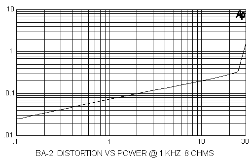
Like the BA-1, the measured performance of both stages together is comparable to that of just the follower output stage. Here is the distortion vs power at 1 Khz into 8 ohms:
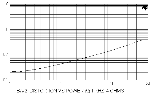
Here is the distortion vs. power at 1 Khz into 4 ohms:
Here is the distortion vs. power at 1 Khz into 2 ohms:
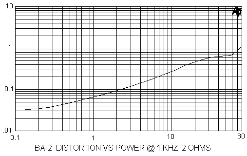
Clearly the BA-2 has far more capacity into low impedance loads than BA-1.
Here is the amplifier frequency response curve at 1 watt:

And here is the distortion vs. frequency:
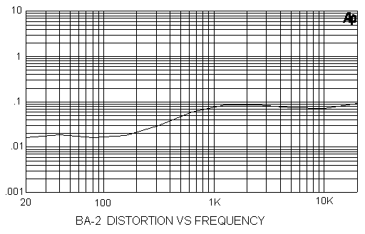
This figure deserves some discussion, as it illustrates the notorious “IR P channel problem” in which the transconductance of the International Rectifier P channel Mosfets exhibit a shelving in the midband. For complementary followers, this shows up as increased second harmonic about about 200 Hz, leveling off around 1 Khz. Is this really a problem? Perhaps it is if you judge by specs, but I have not heard actual complaints from listeners, probably because second harmonic is relatively inoffensive. Here is what the distortion waveform looks like:

There are three common cures to this:
- Use different P channel Mosfets – this problem is specific to IR P channel parts.
- Place the output stage in a feedback loop to correct it.
- Use these circuits in balanced output stages, where the second harmonic will cancel.
Correcting this issue with one or more of the above will reduce the mid to high frequency distortion by about half or more, depending on which cures you pick.
Or you can say, “My, that lovely second harmonic certainly warms up the midrange on cold winter nights.”
Under “miscellaneous”, the measured damping factor of the amplifier came in at about 50 (an output impedance of 0.16 ohms). The noise was about 100 uV at the output, and the balanced input Common Mode Rejection Ratio (CMRR) was about -50 dB.
The Sound
The sonic signature of this sort of circuit is familiar to me after many years of playing with variations on it. It's noted for a warm characteristic and a slightly soft top end. Both the BA-1 and BA-2 have a lineage that goes back to the A75 amplifier from 1992, and they sound a bit like it.
The BA-1 is a little better sonically at low power levels, but is not as capable of being scaled to higher power levels or driving low impedance loads. By contrast the BA-2 can be biased at lower levels if necessary, and can drive low impedance loads without burping. The BA-2 is a little bit softer at the top, and the BA-1 has a tad more detail at the top.
Both sound very good, and if you spend enough time with them, the warmth and soft top end might tend to spoil you for other solid state pieces, so if you have a lot of money invested in the L word, or the K word, or the H word, maybe it's best not to know.
The BA Variations
Before publication, I have received several requests for clarification and expansion:
It's obvious that for the follower designs we can create a front end independent of the main amplifier. As the quarters are tight in the BA chassis, this is a good idea, as it will allow placement away from the noisy power supply and give us considerable flexibility in switching out different circuits without having to take the amp apart. As I said, most of the BA designs will be followers without feedback, so you should feel free to go this route. Variac refers to these as BAGS. I forget why.
The gain of this front end is set at about X 6, or 15 dB. You can have higher gain simply by changing R203 and R204 to higher values. You can double the gain (to about 20 dB) by increasing these to 100 Kohm, and you can push it to 150 Kohm (about 23 dB) without changing the compensation capacitors.
Any more and we might have to apply for a THX sticker. *
You can certainly build this amplifier with fewer output devices as mentioned earlier. It will alter the spectral balance slightly – more outputs tends to put a little more emphasis on the bottom end, and fewer tends to brighten the top. At least this is how you will tend to perceive it. I leave it to you to try this if you like, but I think the direction you would want to go is 2-3 pairs, as we already have overkill with 4.
I have shown a recommended value for the output stage bias at 250 mA / device which is only about 6 watts per device with a +/-25 volt supply. If you have enough heat sinking, you can consider as high as 30 watts per device, allowing the reliable use of fewer devices.
If you decide to higher, remember that Mosfets are better at higher current until they catch fire and fulfill the promise of the amplifier's name.
The supply voltage range is limited by the voltage ratings of the front end Jfets. 35 volts is about as far as you dare go, and 30 volts is the recommended maximum. Any more and you will have to cascode the P channel devices (not so difficult) and increase the value of R205 to 15 or 20 Kohms, otherwise it should work fine.
Less than 18 volts is really not recommended as it starts taking too much out of the circuit's performance (in my humble opinion).
Regulating the supply is a perfectly good idea, and will lower the noise figure slightly. I recommend some nice big capacitors to ground after the regulators to help avoid interaction between the amplifier and regulator circuits.
And yes, there are capacitors in the circuit. One is even employed to form the dreaded bootstrap on the voltage gain stage.
Get over it. **
As always, you are invited to share your experiences in the thread Burning Amplifier #2 discussion thread here on diyAudio.
* that's a joke - I say that's a joke, son...
** Not a joke.
Nelson Pass
© Nelson Pass 2009
You might be interested to know that...
- A limited number of Burning Amp PCBs are available in the diyAudio Store!
- This article is also available as a PDF - download from here
- We're looking for more articles! Do you have an article that would be of interest to diyAudio members? Let us know!
Last edited by a moderator:
Could be anything, but most likely the C5200 and A1943 are too fast as compared to MJ15003/4, thereby causing high frequency oscillation. The bias levels may be different for C5200/A1943, causing overheat, but the heat would build up gradually though.
Anyway, more information is required for the more experienced forum members to help you.
Anyway, more information is required for the more experienced forum members to help you.
It looks like the output stage diagram is not correct. The output signal from the input stage that goes to the 'D' connection of the output stage will not be fed tot he Gate of the MOSFET's, but it will go to the V+ (through C1 and R26), V- through R25 and P2.
Please verify.
Please verify.
- Status
- This old topic is closed. If you want to reopen this topic, contact a moderator using the "Report Post" button.