Hi there,
First, i'm not well versed in electronics, especially digital stuff.
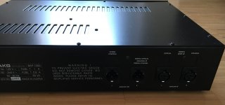
I have a AKG BAP 1000, which is a digital headphone processor from the early 90s. Unfortunately the "digital" only refers to the internal processing. The in- and outputs are analog only (symetrical). However, there are holes and labels for digital input and output, each optical and coaxial on the back of the device and the motherboard has a pair of jumpers labeled DIO and not DIO (which could mean DigitalIO). An AKG employee told me, that a digital IO Upgrade was planned at the time but never released.
My question: Is it in principle possible, to retrofit digital input and output (optical or coaxial) to the device?
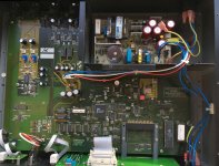
I don't have circuit diagrams, but i'm trying to get them from AKG. The DA converters are Burr Brown PCM56P, the AD converter is a Burr Brown PCM78, all are mounted on sockets. If required i can upload a photo of the motherboard.
Thanks in advance for your help and greetings from Wiesbaden, Germany,
Manfred
First, i'm not well versed in electronics, especially digital stuff.
I have a AKG BAP 1000, which is a digital headphone processor from the early 90s. Unfortunately the "digital" only refers to the internal processing. The in- and outputs are analog only (symetrical). However, there are holes and labels for digital input and output, each optical and coaxial on the back of the device and the motherboard has a pair of jumpers labeled DIO and not DIO (which could mean DigitalIO). An AKG employee told me, that a digital IO Upgrade was planned at the time but never released.
My question: Is it in principle possible, to retrofit digital input and output (optical or coaxial) to the device?
I don't have circuit diagrams, but i'm trying to get them from AKG. The DA converters are Burr Brown PCM56P, the AD converter is a Burr Brown PCM78, all are mounted on sockets. If required i can upload a photo of the motherboard.
Thanks in advance for your help and greetings from Wiesbaden, Germany,
Manfred
Hi,
I found this rather old thread because I also look for a way to get access to the BAP1000 DSP feeding a digital input signal.
rfbrw was so kind to offer support.
For everyone interested I am posting some images of the inside.
Thank you!
Best regards
Michael
I found this rather old thread because I also look for a way to get access to the BAP1000 DSP feeding a digital input signal.
rfbrw was so kind to offer support.
For everyone interested I am posting some images of the inside.
Thank you!
Best regards
Michael
Attachments
-
 01_BAP1000_Analogue input section_small.jpg403.3 KB · Views: 215
 -
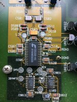
 10_BAP1000_crystal and DiO Jumper_small.jpg424.2 KB · Views: 75
 -
 09_BAP1000_digital processing section2_small.jpg418.1 KB · Views: 75
 -
 08_BAP1000_digital processing DSP section_small.jpg796 KB · Views: 85
 -
 07_BAP1000_digital processing section_small.jpg621.8 KB · Views: 99
 -
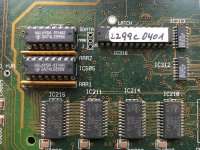 06_BAP1000_RAM section_small.jpg791.9 KB · Views: 88
 -
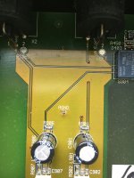
 05_BAP1000_Headphone Output amplifier section_small.jpg452.7 KB · Views: 202
 -
 04_BAP1000_Register section_small.jpg521.6 KB · Views: 206
 -
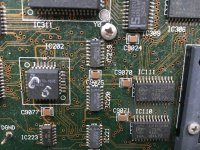
 03_BAP1000_AD converter section_small.jpg502 KB · Views: 210
 -
 02_BAP1000_Analogue input buffer section_small.jpg307.4 KB · Views: 208
...and more...
Sorry, forgot to make an picture of the full PCB...hope the map helps.
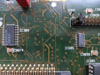
I am wondering if there is a way to make use of the jumper next to the crystal and the pinhead connector (jumper in place) to insert I2S signals from a SPDIF receiver chip.
Would be great to get it working. Unfortunately I could not get any supporting material from Harman nor the former Audio Pro distributor in Germany.
Thanks!
Michael
Sorry, forgot to make an picture of the full PCB...hope the map helps.
I am wondering if there is a way to make use of the jumper next to the crystal and the pinhead connector (jumper in place) to insert I2S signals from a SPDIF receiver chip.
Would be great to get it working. Unfortunately I could not get any supporting material from Harman nor the former Audio Pro distributor in Germany.
Thanks!
Michael
Attachments
-
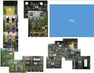 AKG BAP1000 Picture Map.jpg64.8 KB · Views: 90
 -
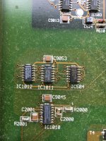
 14_BAP1000_Analogue output filter buffer section_small.jpg416.5 KB · Views: 78
 -
 13_BAP1000_DA Converter section_small.jpg550.6 KB · Views: 65
 -
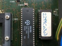 12_BAP1000_ Card and EPROM_small.jpg451.3 KB · Views: 62
 -
 11_BAP1000_ DiO connector with Jumper_small.jpg457.9 KB · Views: 78
Hi,
not sure if I understood your comment correctly.
The Digital-Input card is mounted to the backside of the enclosure and will cover a part of the PCB populated with the analogue input and output stages. There are no other free pin connectors than the one shown on the picture close to the Dio jumper.
The slot-in on the front right is for reading chip cards featuring personal HRTF data measured at AKG lab.
Thanks
Michael
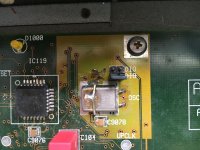
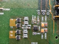
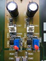
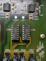
There seems to be more than one version. The pictures I saw had a different ADC and covered up holes at the back for additional digital inputs.
Back to your pictures. One possible approach would be to switch between the ADC and the DIR. Next to the CS5338 ADC is a pad marked 384Fs. Is there another oscillator in addition to the one near the pad marked UPCLK ? I think UPCLK might be the microprocessor clock.
Back to your pictures. One possible approach would be to switch between the ADC and the DIR. Next to the CS5338 ADC is a pad marked 384Fs. Is there another oscillator in addition to the one near the pad marked UPCLK ? I think UPCLK might be the microprocessor clock.
Hi,
yes, you are right. I have the later version with the single overload input LEDs. In the first version there were two multi color LED columns (green, orange, red if I recall correctly). Not sure what the differences are but mine has also covered openings in the back for the Digital input card labeled SPDIF Coax and Toslink.
I checked the inside again but there is no other oscillator...at least on the top side.
I made some additional pictures.
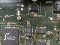
According to the CS5338 data sheet the A/D sends output data L/R, SCLK & SDATA. Looks like they are marked on the board (L/R Pin14, SCLK Pin15 is BCK, SDATA Pin16 is DATA). Do you think I could feed in data here?
Not sure what IC502 is doing.
Thanks
Michael
yes, you are right. I have the later version with the single overload input LEDs. In the first version there were two multi color LED columns (green, orange, red if I recall correctly). Not sure what the differences are but mine has also covered openings in the back for the Digital input card labeled SPDIF Coax and Toslink.
I checked the inside again but there is no other oscillator...at least on the top side.
I made some additional pictures.
According to the CS5338 data sheet the A/D sends output data L/R, SCLK & SDATA. Looks like they are marked on the board (L/R Pin14, SCLK Pin15 is BCK, SDATA Pin16 is DATA). Do you think I could feed in data here?
Not sure what IC502 is doing.
Thanks
Michael
Attachments
Thank you!
I found on Ebay DIR modules called DIR9001 DIR9001 module coaxial / fiber receiving I2S output 24bit 96khz | eBay that support 16bit I2S mode (16bit right-justified) or 24bit (I2S). Next to the output 256Fs is printed on the board. Not sure if one of these modes match.
If it would match is it just connecting to the corresponding landing spots close to the ADC and whatever provides a signal (ADC or DIR) will get data to the DSP?
Thanks
Michael
No, that won't do unless you plan a radical redesign of the unit. You have two devices that both want to be master. The ADC receives all its clocks from the following circuitry so you have MCLK at 384Fs, LRCLK and BCLK as outputs. The DIR extracts MCLK from the SPDIF datastream and derives its clocks from that. MCLK, LRCLK and BCLK are all outputs leaving you with two devices trying to connect to each other with all outputs and no inputs. The way around this is to pick a more flexible DIR, one that will generate MCLK at 384Fs and has a digital audio interface configurable as an input for LRCLK and BCLK. When selected, it can then be clock master by driving the rest of the BAP1000 with its MCLK, hence the need to find the source of the 384Fs clock sent to the ADC. But before we get too far ahead, there is a possible cloud on the horizon and that is FSYNC.
If it is simply connected to V+ then all is good but if it is used we will we have to find another way in. This task is not unlike adding as digital input to a CD player. I've seen a number of schematics for doing that and I always used to think using an ASRC was cheating. Not anymore.
If it is simply connected to V+ then all is good but if it is used we will we have to find another way in. This task is not unlike adding as digital input to a CD player. I've seen a number of schematics for doing that and I always used to think using an ASRC was cheating. Not anymore.
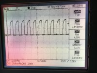
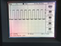
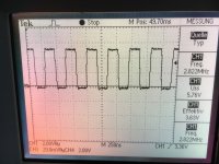
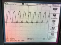
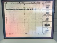
I checked a couple of test points and made "screenshots" of my scope.
Sorry, forgot to switch Scope UI language:
Quelle: Source
Uss: U pk-pk
Effektiv: RMS
1) 384*FS : 16.89MHz guess that's FS=44.1kHz
2) BCK: 2.822MhZ squares
3) DATA: no input 707kHz
4) FSYNC: 88.1kHz --> I guess these are "clouds" right?
5) L/R: 44.1kHz --> would be great if this would be the internal Fs, direct CDA material
6) UPCLK: 2.118 Mhz
Does this make sense?
Thanks!
Attachments
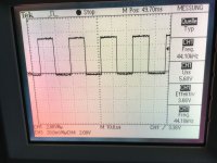
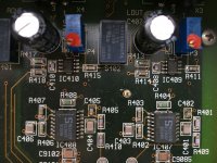
Excellent. So far so good. Spent sometime with the CS5338 datasheet and the evaluation board datasheet attached. See what is going on with FSYNC more clearly now, so it should not be a problem. Nearly time to draw up a schematic, just need to know the voltages at a few pins. I have made an assumption based on the pictures but now need to know for sure.
The pins are,
Pin12 CMODE
Pin13 SMODE
They are both on IC501 CS5338.
The pins are,
Pin12 CMODE
Pin13 SMODE
They are both on IC501 CS5338.
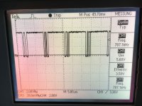
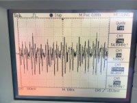
thank you so much diving into it...
here are the scope pics from
1) CMODE Pin12: looks like noisy 5V - CMODE should be tied high to select an ICLKD frequency of 384 X the output word rate.
2) SMODE Pin13: looks like noisy DGND (is also connected to pin 11 TST) SMODE
should be tied low to select serial interface slave mode, where SCLK, FSYNC and L/R are all inputs.
Slave mode...as you have expected.
Thank you!
Michael
Attachments
I have not planned to make it a big effort for you...thank you so much.
BTW I have played a bit with the DIO jumper. If I change it to DIO (active, not striked out) none of these signals above show up at the pads close to the ADC. Does this mean the DIO board acts as master?
BTW I have played a bit with the DIO jumper. If I change it to DIO (active, not striked out) none of these signals above show up at the pads close to the ADC. Does this mean the DIO board acts as master?
- Home
- Source & Line
- Digital Source
- AKG BAP1000 Digital IO