It would depend what is required. Is there a need for a PCB ? Is veroboard and SMT-to-DIL adaptors acceptable ? If it was me, I'd keep it simple and use a Xilinx XC9572XL, it has 5V tolerant I/O and a WM8804 both on a small 2-layer PCB.
Ok, I believe this is the best idea so far, requiring only one chip. I have access to a PIC development board, I read it can program the Xilinx? Where can those SMT-to-DIL adaptors be found for the chip? (I am in Europe).
I suppose everything is made clearer in time, but I also wonder what to do with those non data bits on the left that the JP sends according to the page you referenced. I2S works with those extra bits included? Very confused why those extra bits are on the stream at all.

Ok, I believe this is the best idea so far, requiring only one chip...
"XCX9572L... and a WM8804" is two chips. You might want to read the documentation for XC9572L. From looking at this: Solved: Getting Started with XC9572XL Development Kit - Community Forums ...it would suggest the part is programmed in the same Languages as FPGAs: VHDL or Verilog.
Regarding the diagram above, and the correct protocol and number of bits for your dac chip, rfprw said your it is configured for, "16 or 18 bit LSB/Right justified." The two modes are not mutually compatible, if you choose the wrong one it won't work properly. Examining dac clock frequencies with a scope should give you a certain answer.
Last edited:
"XCX9572L... and a WM8804" is two chips. You might want to read the documentation for XC9572L. From looking at this: Solved: Getting Started with XC9572XL Development Kit - Community Forums ...it would suggest the part is programmed in the same Languages as FPGAs: VHDL or Verilog.
Regarding the diagram above, and the correct protocol and number of bits for your dac chip, rfprw said your it is configured for, "16 or 18 bit LSB/Right justified." The two modes are not mutually compatible, if you choose the wrong one it won't work properly. Examining dac clock frequencies with a scope should give you a certain answer.
Looks like the JP is in the high/high mode (e.g. 18 bits parallel), as at least there is something going to the respective pins (high > 0.7 V).

But I am wondering a few things.
- Are there more bits of audio to the left side of the MSBs that could be used?
- Is the amount of the bits to the left side constant?
- Why/what are the extra bits to the left on the stream in the first place?
And what should the location of those extra bits be in the output I2S stream?
The data sheet also details a configuration where the clock stops during the extra bits. How likely is this scenario - did rfbrw rule it out already?
rfbrw said:The setup for the JP-8000, chart 4, is 18 bit data clocked in in parallel.
I do not have an oscilloscope available at the moment. I would like to leave opening the unit to after the board is done if possible.
Thank you again for the information. Apologies if the questions are too much of a newbie questions. If I was a professional I would not be asking.
Last edited:
For standard RJ PCM there are no extra data bits. The MSB for each channel is sent last, LSB first. The Frame clock up and down edges indicate when left and right channels are alternated. For 18-bit stereo there should be a total of 36 data bits per frame clock period, 18-bits times 2-channels.
Pins 1 and 3 are configuration pins. Their state is permanent unles a change in configuration is required. They set the operational configuration of the DAC. In this case pulling pin 1 high by connecting it to V+ configures the DAC to accept left and right channel data on a pin each (L=pin15 & R=pin14). Connecting it to ground (low) would configure the DAC to accept left and right data in serial on one pin (L and R on pin15). Pin3 configures the word length. 16 bits for low/ground and 18 bits for high/V+.
To the left would be the sample that preceded sample N. Sample N is the current sample. Sample N+1 is the sample to come. Each sample in the case of the JP8000 is 18bits long.
First off, there is no I2S formatted data anywhere in the JP8000. I2S is a data format in its own right but unfortunately some insist on using it as catchall term and the less experienced pick up on this, buy something with I2S in the name and then wonder why it doesn't work.
I2S calls for a specific arrangement of clock and data and that arrangement is not to be found in the JP8000.
At some point datasheets will be referred to and they make no concessions on this topic. I2S will just be one of a number of formats. And I can assure you will find nothing in the datasheet under the name I2S that looks anything like what you will find in the JP8000.
Stopped clock mode would be a function of the source. The only way to know would to use a 'scope.
You can wait until the board is done but the board would be designed based on what would at best be a educated guess or you could proceed on the assumption that JP8080 and JP8000, both use the same DAC, are close enough and the added information the JP8080 schematic is enough.
I would like to leave opening the unit to after the board is done if possible.
Normally, one would want to take a close look of what you will have to attach wires to and where those wires will go. PCM/I2S/DSD signals using the same 3-wire bus structure cannot be transported more than a total of a few inches. You would have to decide on a place to put your little board inside the case that is close enough to the dac and decide a way to mount it. Once you know the physical requirements for you board design you can plan on making it the size and shape it will have to be to work.
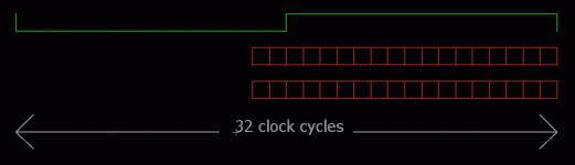
The empty part of the frame is sometimes used for other data as the data does not fill the frame which is typically 32, 24 or 16 bits long per channel but it can be as low as one clock cycle per data bit long or as high as 64 bits per channel long. If what holds for the JP8080 holds for JP8000 each frame is 32bits and the sample occupies the last 18 bits.For standard RJ PCM there are no extra data bits.
If you are sending data to a bit-serial multiplier then yes. Otherwise it is MSB first.The MSB for each channel is sent last, LSB first.
The Frame clock up and down edges indicate when left and right channels are alternated. For 18-bit stereo there should be a total of 36 data bits per frame clock period, 18-bits times 2-channels.
In this specific case data is converted on the falling edge of WDCK. As the data is in parallel LRCK is not required define left from right.
Last edited:
Right. I was talking about the output format he will want to end up with for conversion to SPDIF (if it were to be in RJ format). I consider it "standard" in the sense that it is most commonly what we see and which is more similar to I2S.
For the existing PCM signals that will have to be read, I agree fully.
For the existing PCM signals that will have to be read, I agree fully.
Last edited:
The empty part of the frame is sometimes used for other data as the data does not fill the frame which is typically 32, 24 or 16 bits long per channel but it can be as low as one clock cycle per data bit long or as high as 64 bits per channel long. If what holds for the JP8080 holds for JP8000 each frame is 32bits and the sample occupies the last 18 bits.
If you are sending data to a bit-serial multiplier then yes. Otherwise it is MSB first.
In this specific case data is converted on the falling edge of WDCK. As the data is in parallel LRCK is not required define left from right.
The JP8080 manual... genius. Ok, so F_s is 44100, Bclock = 64*f_s, wclock = 2*F_s. The actual output is 88.2 kHz, so indeed the block has a length of 32 samples, 14 extra bits per "block".
The bit depth internally is of course more than 18 bits, so it is possible that even higher bit depth could be achieved, if more of the bits are included...
Last edited:
Not extra samples. Extra bits. Not useful for more audio bit-depth if the dac chip can't support higher than 18-bit depth audio.
Indeed. Fixed!
Decent DAC can get up to 24 bits with SPIDF. USB full 32 bits floating point?
rfbrw said:Alas, Roland have seen fit to give you only 18 bits but at twice the CD sample rate.
But how do you know the first 14 bits are empty and not full of audio goodness?
rfbrw said:Doesn't matter. The DAC would ignore them. It has been setup to convert 18 bits and 18 bits is all it wll convert.
I am a bit confused. The idea is to take the stream from the inputs of the DAC, so why does it matter what the DAC does?
rfbwr said:It is not so much what the dac does. It is what it is configured to accept for conversion.
The sample is 18 bits long.
Ok, if it is so it is so.
Downloading the Xilinx ISE now, so many Gbs and US Government verification. Things are getting serious now.
Dithering to 18 bits... would they even bother wasting cycles on that in the 90s. I guess we will see.
Last edited:
- Status
- This old topic is closed. If you want to reopen this topic, contact a moderator using the "Report Post" button.
- Home
- Source & Line
- Digital Source
- Add a digital out to Roland JP-8000 synthesizer.