Hi Terry,
& thanks for your info ... So that is what AKM mean with the "64 ohm, typical" in the pin function table in the data sheet (??) ... I assumed it meant that the IOUTs should be connected to the relevant OPIN pins via a 64 ohm resistor. So thinking since AKM also write 64 ohms in the text associated with the OPIN pins ...
Anyway, this is food for thought. Currents this high (72 mAs) may almost be the quiescent current of the output transistors of a "normal" output amplifier
Cheers,
Jesper
Hi Terry,
& thanks for your info ... So that is what AKM mean with the "64 ohm, typical" in the pin function table in the data sheet (??) ... I assumed it meant that the IOUTs should be connected to the relevant OPIN pins via a 64 ohm resistor. So thinking since AKM also write 64 ohms in the text associated with the OPIN pins ...
Anyway, this is food for thought. Currents this high (72 mAs) may almost be the quiescent current of the output transistors of a "normal" output amplifier
Cheers,
Jesper
Not a huge surprise, ES9038PRO is like this, too. To achieve the crazy SNR specs they parallel a lot of DACs and then let you figure out how to best handle it.
Hi Terry,
& thanks for your info ... So that is what AKM mean with the "64 ohm, typical" in the pin function table in the data sheet (??) ... I assumed it meant that the IOUTs should be connected to the relevant OPIN pins via a 64 ohm resistor. So thinking since AKM also write 64 ohms in the text associated with the OPIN pins ...
Hi Jesper,
No probs. Actually the DAC OP should be connected directly to a virtual ground with, ideally, zero voltage swing.
These DACs (Sabre same) are really masses of parallel high value resistors switching between Vcc and Gnd via internal logic gates. So in the AKM's case that 64 ohms is the sum parallel value of all the resistors.
To be able to achieve 140dB dynamic range (mono mode) means a LOT of parallel resistors to get johnston noise down and OP current swing up.
One would assume they must be getting close to what is achievable in a chip.
Anyway, this is food for thought. Currents this high (72 mAs) may almost be the quiescent current of the output transistors of a "normal" output amplifier
Or you can look at it like +-37mA. There are opamps that will do it, but also achieving the distortion spec is certainly a formidable challenge. it will be interesting to see full data sheet and exactly what they used to get the numbers.
cheers
Terry
Hi again ...
@Terry: Thanks for elaborating. Well, I suppose it helps to consider it as +/- 37 mA swing - but my, my - that really is a lot. And since I admittedly am not that much into using opamp in the sound circuitries this likely will be a challenge ... Anyway, still amazing that they are able to get such specs.
@chris719:
...
But somewhere in the back of my mind there's a thought that this huge amount of current may actually be an advantage ... I reckon I just have to twist my mind into seeing this.
Cheers,
Jesper
@Terry: Thanks for elaborating. Well, I suppose it helps to consider it as +/- 37 mA swing - but my, my - that really is a lot. And since I admittedly am not that much into using opamp in the sound circuitries this likely will be a challenge ... Anyway, still amazing that they are able to get such specs.
@chris719:
.. Well, yes, it looks like I'm having to think well and maybe long about this ...To achieve the crazy SNR specs they parallel a lot of DACs and then let you figure out how to best handle it.
... But somewhere in the back of my mind there's a thought that this huge amount of current may actually be an advantage ... I reckon I just have to twist my mind into seeing this.
Cheers,
Jesper
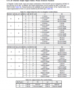
Just in the process of laying out a prototype board for the AK4499 & trying to decide how to configure the outputs.
AKM only show two options.
DAC registry’s configured for mono & all four channels wired in parallel after the I/V stages.
Or with two left & 2 right channel output stages.
I only want to use it in stereo with 2 channel output so what do you think would be the best way to do it?
1. Just use one DAC section leaving the other one unconnected?
2. Use the whole DAC & combine the 2 left & 2 right.
If using option 2 I guess I just parallel the 2 x L & 2 x R after the I/V stages - sound ok?
I was thinking of a third option by possible passively combining each pair of outputs &
then a common I/V stage - a few small value series output resistors to help current sharing.
Anyway just wanted to bounce it of you guys & see what you think.
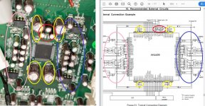
I would build the reference schematic of Fig. 83 of the datasheet, splitting it in half so that the top two outputs get combined into one channel and the lower two channels get combined into the second channel. Then I'd set (in software) the top two channels as Left and the bottom two as Right channel.
1. Just use one DAC section leaving the other one unconnected?
As goes with the AK4490, using a single DAC for each channel:
1. SNR rises as more channel in parallel as more SNR. THD will remain equal.
2. The channel separation would be with the noise floor (seen on RME ADI 2 pro) if proper done
3. The build in FIR may similar to the Ak449x series and the sound will be similar... just a guess.
This means for me, a full mono design per chip would be the target.
I would build the reference schematic of Fig. 83 of the datasheet...
It seams that someone has a better PDF with more pages. In other words: is this one public?
Hp
It seems that also AKM made their test prototype like you said.I would build the reference schematic of Fig. 83 of the datasheet, splitting it in half so that the top two outputs get combined into one channel and the lower two channels get combined into the second channel. Then I'd set (in software) the top two channels as Left and the bottom two as Right channel.
Probably the reference design will be very close to it.
I am a little bit confused about the opposite layout of the MCLK pin vs. I2S pins in the chip.
Attachments
@HpW:
It is now public and can be downloaded from AKM's webpages without any need to sign up for anything. Link is here:
https://www.akm.com/file.jsp?id=600977
Cheers,
Jesper
It seams that someone has a better PDF with more pages. In other words: is this one public?
It is now public and can be downloaded from AKM's webpages without any need to sign up for anything. Link is here:
https://www.akm.com/file.jsp?id=600977
Cheers,
Jesper
The structure is very amateurish. The output lines couple with the power lines.It seems that also AKM made their test prototype like you said.
Probably the reference design will be very close to it.
I am a little bit confused about the opposite layout of the MCLK pin vs. I2S pins in the chip.
It seems that also AKM made their test prototype like you said.
Probably the reference design will be very close to it.
I am a little bit confused about the opposite layout of the MCLK pin vs. I2S pins in the chip.
Yes, that design choice is annoying. Input signal routing will definitely require compromises to be made.
Btw, I hear that there also exists a datasheet for the official evaluation board. But I have not been able to find it.
It is interesting that in the data sheet they show 2200uf for the VREF cap but on the Eval board schematic it shows 2 x 220uf & in the photo of the Eval board it looks like a single 470uf is used. It is obviously a critical area & they tried various options. Also on the Eval board schematic there are 10 ohm resistors is series with the VREF pins on the chip. Any ideas on those?
There's a bit about it on page 108 of:
https://www.akm.com/file.jsp?id=600977
from gentlevoice's post 55 above (Thanks!), section '10.3. Reference Voltage'. Not sure if that entirely answers your question, but it does look like it was an issue that caused them some grief.
Regards,
Rick
https://www.akm.com/file.jsp?id=600977
from gentlevoice's post 55 above (Thanks!), section '10.3. Reference Voltage'. Not sure if that entirely answers your question, but it does look like it was an issue that caused them some grief.
Regards,
Rick
The one I downloaded yesterday was 117 pages. You had to sign up to get newsletters and stuff to download it.
Yes, their website is a total mess since they came up with the myAKM garbage. Thanks to Gentlevoice for linking it directly
.- Status
- This old topic is closed. If you want to reopen this topic, contact a moderator using the "Report Post" button.
- Home
- Source & Line
- Digital Source
- AK4497 won't be Flagship anymore