Your reported issues are not normal for a 205. The only "normal" issue in your case, is the headphone oscillations. This stage it oscillate (as usually) in Mhz range, due to design faults in the analogue output section.
I will suggest you, following the Oppo recommendation, and sending it to them for fixing.
I will suggest you, following the Oppo recommendation, and sending it to them for fixing.
Thanks for the reply.
I did test the outputs with and without loads. The stereo RCA outputs are normally cabled directly to the inputs of an Aragon 4004 Mk II power amp. I looked at the headphone outputs with three different loads: 120 ohm resistors, connected to the power amp, and connected only to the scope. The loadings don't substantially change the HF garbage that I reported in the previous post.
There was a problem with the jack-to-RCA adaptor that I used for testing the headphone port. After fixing that, I measured an even larger oscillation in both headphone channels: 150mV p-p at 45 MHz, and amplitude modulated at about 600kHz.
I am not disappointed by this UDP-205. The sound quality is pretty damn fine, and I am listening through very revealing full-range electrostatic speakers (Acoustat 3). If I had to name a flaw, I might wish for a slight improvement in the depth of the stereo imaging. I don't know if a fix for the HF garbage would improve that, or any other aspect of SQ.
Did you try to mute the outputs by pressing the mute button on the remote or turning the Oppo volume down to its absolute minimum value and measured the output?
Did you try to mute the outputs by pressing the mute button on the remote or turning the Oppo volume down to its absolute minimum value and measured the output?
Yes and yes. The oscillations on the outputs were not affected.
When you mute the outputs (and also I believe also when you send a digital zero by turning the volume down to its minimum), the output relays switch to ground, effectively disconnecting from the DAC output circuit. This switch to ground, especially on mute is audible by hearing the relays clicking from one tap to another connected to ground. If at this stage you still get oscillations on the outputs, then I believe the problem is a simple replacement of the relays, imho.
Yes and yes. The oscillations on the outputs were not affected.
Try loading the RCA's right at the connectors, with something like 500 ohms, i.e. remove the interconnects' length and the pre-amp input impedance from the equation. The noise you reported is of a very high frequency; very unlikely that it would be coming via analog output stage signal path. There's capacitive/inductive coupling happening somewhere, from the (most likely) noisy ground..??
What happens if you place the probe hot at the output RCA's ground pin, and probe ground at the main DC rails' filtering capacitors "zero" / "return" ground point?? What is the amount of measured noise then? Make sure that the probe ground lead is thick, braided copper wire type.
I think the ground uniformity might be the root cause here...
The unit was shipped off to Oppo's service center on Friday, so I can't do any more tests myself. I don't see how changing my probe setup is relevant. I did try changing cables, loads, connecting to different inputs of the scope, etc. The same pattern was always seen. Only one of the RCA outputs showed oscillation - all the others were clean. The HF garbage from the left channel RCA output propagated through my power amp, all the way to the output. Right channel clean.
The headphone outputs showed HF garbage no matter what I tried. I suspect unstable op-amps and/or faulty grounding or decoupling.
The headphone outputs showed HF garbage no matter what I tried. I suspect unstable op-amps and/or faulty grounding or decoupling.
I don't see how changing my probe setup is relevant.
To do what I suggested, you would probably need to extend a (usually) very short and thin probe ground lead, to reach the reference ground point for measurement; hence the recommendation for an appropriate wire for the job. Since you shipped the player to Oppo, it doesn't really matter.
Please explain how a relay causes oscillation in the MHz. In any case, this UDP-205 is on its way back to the Oppo service center. If they tell me anything of interest, I will post to the group.
Mechanical relays have inductance and capacitance specs, albeit low. Hence if something's malfunctioning (say if it can't fully switch on or off correctly), then a resonant oscillation could possibly happen.
The 25M Mhz clock it run the optical drive decoder/processor, beside it.
The HDMI interfaces are part of the main processor, which is clocked by 27Mhz. In 205 model, HDMI audio dedicated output is processed by its own (SI) processor, clocked by a 27Mhz resonator, in addition of a SAW 148,5 Mhz oscillator.
Will there be any benifit from upgrading the 25 Mhz clock on the 205?
Or os it only the 27Mhz main board and 100 Mhz for the DAC that will give any benifit?
Yes indeed, there is beneficial upgrading all clocks on 205... The 25Mhz clock it run the decoding processor for optical drive. The disks reading and data processing quality it get then improved.
The first upgrading priority are 27/25Mhz clocks, then DAC clock. For DAC clock the most important is the power quality provided at the oscillator power pin. The oscillator in itself is good also as it is for its job.
The first upgrading priority are 27/25Mhz clocks, then DAC clock. For DAC clock the most important is the power quality provided at the oscillator power pin. The oscillator in itself is good also as it is for its job.
Yes indeed, there is beneficial upgrading all clocks on 205... The 25Mhz clock it run the decoding processor for optical drive. The disks reading and data processing quality it get then improved.
The first upgrading priority are 27/25Mhz clocks, then DAC clock. For DAC clock the most important is the power quality provided at the oscillator power pin. The oscillator in itself is good also as it is for its job.
OK, cause by a mistake the 25Mhz was removed as well on the Oppo 205 when upgrading the 27Mhz and the 100Mhz (DAC)
So need either to replace (insert the olde one) or get a new upgrade clock for the 25 Mhz since this has a positive effect as well.
In a previous post (#658) I described HF oscillations on the left channel of the stereo RCA outputs on my UDP-205, and on both channels of the headphone jack. I reported this to Oppo service and they told me to send the unit in for repair.
They replaced the stereo audio board. The service center included a sheet showing their measurements with the old and new boards. Both channels are now clean. Left channel HF noise was reduced by 5x.
Did the fix improve sound quality? Maybe a tiny bit more clarity, but I'm very hesitant to make judgments from listening tests separated by several days.
They did not eliminate the 45 MHz garbage on the headphone channels. It is now even higher in amplitude. Since I rarely use headphones, this is not a worry for me. But it adds credibility to the statements by Coris that this is a design flaw which can't be easily fixed.
Nice work by the service center. Good communications, quick turn-around, and they even included another one of the coveted Oppo-branded black cloth shopping bags.
After my UDP-205 was returned, I messaged Oppo's repair center, asking about the cause of the (unrepaired) HF oscillation on the UDP-205 headphone jack. FYI, here is the text of my message and their reply:
Draw your own conclusions.
Thanks for the quick turn-around. The HF oscillation on the left channel stereo RCA output is gone. But I also reported 45MHz oscillation on both channels of the headphone jack. This is still present, and with the replacement board, the amplitudes are actually greater than before, and larger than music signal levels. It's less of a concern for me, since I rarely use headphones. But I am curious about why it was not fixed. I read a report on the web from someone who thinks that this oscillation is a design flaw in the UDP-205, implying that it is present in all or most units. Can you reply to that? Since the unit is no longer being sold, there's really no reason for not being candid.
We have heard of a similar report regarding the headphone output. The audio board was replaced on your unit, so if two audio boards are showing something similar, it is possibly hardware relate. Wish we had an answer for you, but unfortunately we have not heard back from the Factory Team when we initially inquired about it.
Draw your own conclusions.
Thx. 3A would have your Rcore transformer at its max rating so I see that's the limit of your PSU (for all voltage needs combined).
I have ordered a 203 but it hasn't shipped yet so I'm not yet in a position to look inside the unit itself. (I've also put myself down as interested in a final run of the 205.) What voltages are required to be supplied by the PSU? From heyj's pics I see the 203's analogue board requires +/- 15V but, like him, I wouldn't be worrying about that. Does the digital board only expect 12V? What about the 205?
A year-old post, but has anyone actually measured the 12V DC current draw for 205 digital board while a BluRay disc is spinning and the output is 4K (i.e. at maximum power consumption/dissipation?)
Greetings to all: New member here. Looking for info about Clones Audio Oppo 203 mod before buying. I am thinking of getting the Deluxe version of their Power Supply module for the 203, but I can't seem to find any reviews of it on the web. If anyone has tried it in their Oppo 203, can share experiences/impressions about what difference it made, the input would be highly appreciated.
I use the Oppo 203 as a source for Roon Audio, and, occasionally for CD music, that is why I am curious about what enhancements the Power Supply upgrade might bring. Of course, I also use it for watching blu rays in both 1080p and UHD format, so comments about any possible improvements in video quality would be welcome too. The bottom line is that this a considerable investment for me, so I would like to make sure that the improvements would be worthwhile before taking the plunge.
Thanks.
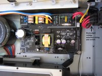
203 power supply does all the rails; +12 for the digital board as well as +15 and -15 for the analog board. Hence, it is important to get it right.
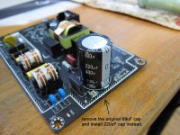
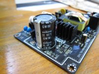
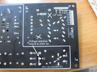
You do not need to spend a few hundred bucks on the ready-made power supply if you can solder... See the attached photos. They are showing the power supply for 205; nevertheless, you'll get the drift. The mods I did for +12V digital board have decreased the noise substantially (10 folds), improved picture (in particular!), but sound as well (I use external 2TB HDD plugged at the back USB port, to play all my content - music and movies. This HDD is powered from the same +12 V digital board' bus...).
What you'll need to do is to use SILMIC II capacitors (instead of OSCONs) for +15 and -15 analog board; do not forget the same smd capacitor combo (10uF + 1uF) on each rail.
The cost of all parts should be below $30 - $40. And.... you can be proud of the mod because you did it yourself.
Attachments
I have also experimented a lot trying the improving of the existing SMPSes for Oppo players. Increasing the capacity of the main cap in the SMPS it was also my first try. Improving the DC output filtering I have tried as well. I have tried many other solutions. Some overall improvements occurred... but best results were only when using a linear power supply.
When Oppo used a quite low capacity (68µF) for main filtering cap in their SMPS, they had a reason: minimising the power the SMPS use when in standby (no load connected). Here it is a compromise in between the lowest ripple current (power use when in standby mode), and the acceptable noise at the SMPS outputs.
As known a SMPS (active power supply), it use power from outlet for its own use, when no loaded. This low but in fact power use it come from its always running oscillator inside (and the control system), and mainly from the (always) ripple current, caused by the main filtering cap. When the capacity of this cap is higher, so it is the ripple current as well.
Let`s say the SMPS, as an always power consumer, it is not a very big issue, as such power is quite low (2-5w). Many such SMPSes all around in a house it mean in the end an important waste... The higher power SMPS is rated, the higher standby consumed power.
Ignoring this waste aspect, it still also (and always) an high HF noise level at an SMPS output, which it propagate further into the powered system, no matter the filtering measures are taken.
Improving the existing SMPS in this case it is possible, but in my opinion an LPS (passive power supply) it is the best solution for dramatically lowering the noise related issues when powering a digital system. An LPS never generate the typical HF noises an SMPs it does. Such noises are to be added to the powered digital system own generated HF noises, and the result it is enough complex and almost impossible to be filtered out. An LPS does not have a such issue. The LPS (fully free HF noises referring to a SMPS noise range), it only dramatically lower the overall noise into the powered digital system.
I am not rejecting the SMPS improvements presented here, obtained with a relative low cost investment. The final result it is also proportional with this involved low cost as well...")
When Oppo used a quite low capacity (68µF) for main filtering cap in their SMPS, they had a reason: minimising the power the SMPS use when in standby (no load connected). Here it is a compromise in between the lowest ripple current (power use when in standby mode), and the acceptable noise at the SMPS outputs.
As known a SMPS (active power supply), it use power from outlet for its own use, when no loaded. This low but in fact power use it come from its always running oscillator inside (and the control system), and mainly from the (always) ripple current, caused by the main filtering cap. When the capacity of this cap is higher, so it is the ripple current as well.
Let`s say the SMPS, as an always power consumer, it is not a very big issue, as such power is quite low (2-5w). Many such SMPSes all around in a house it mean in the end an important waste... The higher power SMPS is rated, the higher standby consumed power.
Ignoring this waste aspect, it still also (and always) an high HF noise level at an SMPS output, which it propagate further into the powered system, no matter the filtering measures are taken.
Improving the existing SMPS in this case it is possible, but in my opinion an LPS (passive power supply) it is the best solution for dramatically lowering the noise related issues when powering a digital system. An LPS never generate the typical HF noises an SMPs it does. Such noises are to be added to the powered digital system own generated HF noises, and the result it is enough complex and almost impossible to be filtered out. An LPS does not have a such issue. The LPS (fully free HF noises referring to a SMPS noise range), it only dramatically lower the overall noise into the powered digital system.
I am not rejecting the SMPS improvements presented here, obtained with a relative low cost investment. The final result it is also proportional with this involved low cost as well...
Last edited:
Recently I got on my bench a 205, with an added Femto clock modification (and Opomod LPS). The device was not functioning at all, not starting up.
I would like to share some of my observations, regarding this modification approach, because such so-called improvement it rises up some serios worries.
First, I would like to point out about the original DAC clock on stereo board. This 100 Mhz oscillator is covered by a shield well soldered to the board. In his installation instructions tutorial for Femto clock board, Oppomod give the impression that it is a requirement for removing the original shield of the DAC clock, to make possible soldering the buffer board connections on points inside the shielded area. More, it is shown in that tutorial that the oscillator itself should be removed, as some other components around. This way of doing is definitely and fully wrong!
The shielding of the DAC clock is very difficult to be removed with the means, and tools of mostly DIY guys, who may think to implement such Femto mod. The chance for catastrophic damages on PCB is very high. Removing this oscillator shield is highly unnecessary!
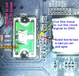
The clock device for DAC it can be very easily isolated and dismissed, by only cutting two traces: 3,3v power supply and clock signal output. Please take a look at the picture bellow.
You can very well and elegant glue somehow the Femto buffer for DAC on the existent shield, and connect directly the ground of the buffer to the shield itself. Then its 3,3v input, to the available 3,3v traces. Also, the output of the Femto buffer it can be easily soldered to the DAC clock input trace (after cutting the connection to the original oscillator).
Well, some magnifier tools may be necessary to succeed in this task, as some fine soldering irons, but is by far much easy than struggle a lot with removing of that shield.
Also pay attention when cutting the traces, to not go too deep into the PCB with your cutting device, as some other traces inside (into) the board it can be damaged so. Just scratch and cut only the copper surface of the trace.
I would like to share some of my observations, regarding this modification approach, because such so-called improvement it rises up some serios worries.
First, I would like to point out about the original DAC clock on stereo board. This 100 Mhz oscillator is covered by a shield well soldered to the board. In his installation instructions tutorial for Femto clock board, Oppomod give the impression that it is a requirement for removing the original shield of the DAC clock, to make possible soldering the buffer board connections on points inside the shielded area. More, it is shown in that tutorial that the oscillator itself should be removed, as some other components around. This way of doing is definitely and fully wrong!
The shielding of the DAC clock is very difficult to be removed with the means, and tools of mostly DIY guys, who may think to implement such Femto mod. The chance for catastrophic damages on PCB is very high. Removing this oscillator shield is highly unnecessary!
The clock device for DAC it can be very easily isolated and dismissed, by only cutting two traces: 3,3v power supply and clock signal output. Please take a look at the picture bellow.
You can very well and elegant glue somehow the Femto buffer for DAC on the existent shield, and connect directly the ground of the buffer to the shield itself. Then its 3,3v input, to the available 3,3v traces. Also, the output of the Femto buffer it can be easily soldered to the DAC clock input trace (after cutting the connection to the original oscillator).
Well, some magnifier tools may be necessary to succeed in this task, as some fine soldering irons, but is by far much easy than struggle a lot with removing of that shield.
Also pay attention when cutting the traces, to not go too deep into the PCB with your cutting device, as some other traces inside (into) the board it can be damaged so. Just scratch and cut only the copper surface of the trace.
Attachments
Last edited:
As I mentioned in above post, the 205 equipped with a Femto clock board I got, it was defective, not starting up.
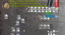
The cause of the issue it was the relay control transistor which it was burned (see picture 7).
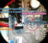
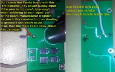
The Femto clock board it is connected as shown in picture, on the relay control pins. VERY WRONG!
This Femto board it takes 300mA on its 5v power input, and the relay control circuit it was not designed to sustain a such supplementary current. The transistor used by Oppo to control the relay it is specified for an absolute max. current of 500mA. The Femto clock board it have also an 10000µF capacitor, which it take an important inrush current at starting up, even though the resistor serial mounted to it.
The total inrush current it overloads the relay control transistor, and its life span it shorten drastically. The marked “+5v “, nearby the power connector pin, it is not meant to source 5v other than to the relay itself. This pin is not a +5v power supply! This important consumer (300mA) it also overloads the SMPS which it primary provides this power.
Another risky situation when installing this kit, it is the 5v connection in itself as it is advised in the installation tutorial (see picture 8).
This Femto clock board it should be powered from elsewhere than the main board. But in such case, power up synchronising it should be solved…
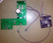
More about the ” engineering” approach in this Femto clock case…
Femto clock approach/kit (picture 1) it is based on an PLL chip which it is run it by a 40Mhz oscillator, and it provides differential outputs for different clock signals. On a second PCB in this kit, it is installed an 25Mhx oscillator, powered by a 3,3v regulator, to provide clock to the optical drive processor. The differential line transmissions coming from the Femto chip itself, are converted to unbalanced output by a buffer chip. This buffer chip mounted on a small PCB, it has to be powered by 3,3v.
Oppomod tutorial advise connecting the 3,3v buffer board (27Mhz clock) power pin, directly to the small SMPS on main board. One can only imagine what HF noise level is injected in this way, into the clock signal for main processor… Femto clock approach is meant to improve the clock system for this device…
The Femto kit board which it has installed the 25Mhz oscillator it has also a very professional solution for +5v connection to the board (see picture 3). Maybe such connection it lowered drastically the production costs…
Another issue I can see about the 27Mhz clock signal output, is its TTL level. This TTL clock signal level is meant (in the conception of the Femto clock producer) to get so into the main processor clock pin input (see picture 5), which it was designed for a LVDS level…
LVDS signal level is much lower than the level provided by the buffer. I appreciate as very risky injecting a such high-level signal into the processor input which it was not designed to sustain a such high level. It may work for a while…
The same situation is about the DAC 100Mhz clock signal. But here, fortunately the ESS9038 it tolerates TTL signals at its clock input…
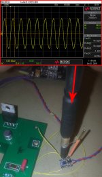
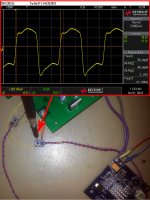
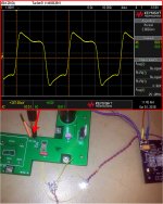
I added hereby for your appreciations, the measurements taken on all of the clock outputs of Femto kit. Jitter is not measured...
The cause of the issue it was the relay control transistor which it was burned (see picture 7).
The Femto clock board it is connected as shown in picture, on the relay control pins. VERY WRONG!
This Femto board it takes 300mA on its 5v power input, and the relay control circuit it was not designed to sustain a such supplementary current. The transistor used by Oppo to control the relay it is specified for an absolute max. current of 500mA. The Femto clock board it have also an 10000µF capacitor, which it take an important inrush current at starting up, even though the resistor serial mounted to it.
The total inrush current it overloads the relay control transistor, and its life span it shorten drastically. The marked “+5v “, nearby the power connector pin, it is not meant to source 5v other than to the relay itself. This pin is not a +5v power supply! This important consumer (300mA) it also overloads the SMPS which it primary provides this power.
Another risky situation when installing this kit, it is the 5v connection in itself as it is advised in the installation tutorial (see picture 8).
This Femto clock board it should be powered from elsewhere than the main board. But in such case, power up synchronising it should be solved…
More about the ” engineering” approach in this Femto clock case…
Femto clock approach/kit (picture 1) it is based on an PLL chip which it is run it by a 40Mhz oscillator, and it provides differential outputs for different clock signals. On a second PCB in this kit, it is installed an 25Mhx oscillator, powered by a 3,3v regulator, to provide clock to the optical drive processor. The differential line transmissions coming from the Femto chip itself, are converted to unbalanced output by a buffer chip. This buffer chip mounted on a small PCB, it has to be powered by 3,3v.
Oppomod tutorial advise connecting the 3,3v buffer board (27Mhz clock) power pin, directly to the small SMPS on main board. One can only imagine what HF noise level is injected in this way, into the clock signal for main processor… Femto clock approach is meant to improve the clock system for this device…
The Femto kit board which it has installed the 25Mhz oscillator it has also a very professional solution for +5v connection to the board (see picture 3). Maybe such connection it lowered drastically the production costs…
Another issue I can see about the 27Mhz clock signal output, is its TTL level. This TTL clock signal level is meant (in the conception of the Femto clock producer) to get so into the main processor clock pin input (see picture 5), which it was designed for a LVDS level…
LVDS signal level is much lower than the level provided by the buffer. I appreciate as very risky injecting a such high-level signal into the processor input which it was not designed to sustain a such high level. It may work for a while…
The same situation is about the DAC 100Mhz clock signal. But here, fortunately the ESS9038 it tolerates TTL signals at its clock input…
I added hereby for your appreciations, the measurements taken on all of the clock outputs of Femto kit. Jitter is not measured...
Attachments
Last edited:
- Home
- Source & Line
- Digital Source
- Oppo new UDP series players - 203/205 - Discussions, upgrades, modifications