Hi Jesper - you could start with this brief from Maxim. They're called 'SAR' ADCs btw.
Understanding SAR ADCs: Their Architecture and Comparison with Other ADCs - Tutorial - Maxim
Understanding SAR ADCs: Their Architecture and Comparison with Other ADCs - Tutorial - Maxim
Hi All,
Thanks for your feedback ;-) - I'll look into it ...
@abraxalito:
Just thinking ... might one of you know of a practical schematic so that I could take a glance at how such an ADC is actually implemented?
Thanks again")
Jesper
Thanks for your feedback ;-) - I'll look into it ...
@abraxalito:
... I was actually wondering if this was what it was called when an ADC instead of a DAC.Hi Jesper - you could start with this brief from Maxim. They're called 'SAR' ADCs btw
Just thinking ... might one of you know of a practical schematic so that I could take a glance at how such an ADC is actually implemented?
Thanks again
Jesper
Hi All,
Thanks for your feedback ;-) - I'll look into it ...
@abraxalito:
... I was actually wondering if this was what it was called when an ADC instead of a DAC.
Just thinking ... might one of you know of a practical schematic so that I could take a glance at how such an ADC is actually implemented?
Thanks again
Jesper
A long time ago, used a 74HCT393 4-bit binary counter's output to make an analog-output staircase waveform generator.
I don't have a good schematic but the description is simple.
First, I placed an opamp near the overall output, to buffer and sum the DAC's outputs, to make the final analog output signal. To form the signal for the (non-inverting) op amp amp's input, I first put a resistor to ground from the op amp's positive input; call it Rin (and configured the op amp's feedback and negative input network etc for the gain I wanted). Then I placed a resistor with value Rdac (given below) between the 8s bit (digital bit 4 of 4) digital output and the top of Rin, and 2 x Rdac from the 4s bit output to the top of Rin, and 4 x Rdac from the 2s bit output to the top of Rin, and 8 x Rdac from the 1s bit output to the top of Rin.
You can see that it forms a weighted voltage-divider summing network, with voltage-divider weightings that are powers of two (or should be).
I believe there is some simple equivalent multistage R-2R resistor network configuration that makes the same thing as my 8R-4R-2R-R (and some Rin) network.
For some reason, I used 50k for Rin and made Rdac 250k. Today, I would probably try to use smaller values.
In my circuit's case, I also put a small resistance (in the 50 to 400 Ohms range, to fine-tune the total resistance value for each bit) between each digital output and its main DAC resistance, and also added a small cap to ground after each small resistance (1000 pF to 2200 pF), to fine-tune the rise-times and edge shapes.
It worked well. It was for a test instrument (stimulating transistor base or gate), not audio, although I ended up running it in the step-rate range from 30 Hz to 22 kHz, and thus the very nice stair-step edges had frequency components much higher than that. (The DAC output op amp amp's output went to a step attenuator, and the attenuator's output went to a selectable inverting amp and then to an Improved Howland Current Pump op amp amplifier, with a small two-transistor push-pull power amplifier (BD-139/140) inside the Howland's feedback loops, which had an overall output that could be configured with a switch (100 Ohms to ground or not) so that it could produce either voltage steps or current steps, with a peak output of +/-15 Volts at +/-1.5 Amps (barely) into 10 Ohms.)
Last edited:
@abraxalito:
Hi again ... no I don't mean a transistor schematic but maybe if there were a schematic with actual components used, i.e. ICs etc. it could be interesting to see a practical implementation.
@georgehifi: Thanks for the reference ... yet in this case I'm looking to see how it might be done in practice ...
@gootee: Thank you also for outlining your approach. I'll see if I can put it into a schematic for visualizing it one of these days.
Greetings to you ;-)
Jesper
Fig1 in the link I posted shows a block diagram. Do you mean you want a transistor level schematic of that? If so I don't hink its going to happen...
Hi again ... no I don't mean a transistor schematic but maybe if there were a schematic with actual components used, i.e. ICs etc. it could be interesting to see a practical implementation.
@georgehifi: Thanks for the reference ... yet in this case I'm looking to see how it might be done in practice ...
@gootee: Thank you also for outlining your approach. I'll see if I can put it into a schematic for visualizing it one of these days.
Greetings to you ;-)
Jesper
Back in the 70's my first computer display was a bunch of resistors soldered to a 2 x 8-bit parallel output port, forming two R-2R ladders, one feeding the X channel of my oscilloscope, the other the Y channel. Just a little bit of assembler code, and Robert was my father's brother...A long time ago, used a 74HCT393 4-bit binary counter's output to make an analog-output staircase waveform
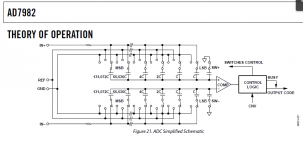
Page 7 (typical applications) of this DS has some real component (IC) names for a 12bit SAR ADC - http://www.classiccmp.org/rtellason/chipdata/mm74c905.pdf
Hi again,
Thanks once more for your feedback ... I'll look into them.
BTW making a sudden search at linear's webpages I came across this description in their AN-17:
http://cds.linear.com/docs/en/application-note/an17f.pdf
... and also in their LT1016 datasheet there's an example of an SAR converter.
So - with the input you have given - I reckon I have the information I have been looking for for now.
Thanks again,
Jesper
I tried something like that today, though I didn't use the complete R2R-network, since it was only supposed to be a proof of concept to show my professors how I thought this could be built. Instead, I used a regular resistor-ladder.
I used 4 OpAmps to build a 2-bit decoder, where one was required as unity gain buffer.
After the unity gain buffer, I had a simple Comperator. Then, I subtracted half the comperators output from the signal. After that, a second comperator followed (at a lower Voltage). The output of the comperator supplied two LEDs.
Theory of operation: As long as the signal is below the level of the first comperator, the signal is presented as is to the second comperator. Therefore, increasing the voltage, the second LED is connected first.
Once the Voltage increases above the level of the first comperator, the first LED is connected and half the Voltage is subtracted from the signal. The second LED is shut down.
Increasing the voltage further, (signal - [first comperator]) is big enough to trigger the second comperator again: Both LEDs are glowing.
However, this circuit would require very precise OpAmps, which have to reach their V+ and V- precisely. Furthermore, any succeeding bits would require different weighing of subtraction and therefore different resistors, all of them to a high degree of precision.
Is there some kind of online scematics editor, so I can show you the exact layout? Perhaps you can find a way around the problem with subtraction ...
Until then, here is a rough schematics of my circuit:
Succeeding bits would get the subtraction output as signal!)
I used 4 OpAmps to build a 2-bit decoder, where one was required as unity gain buffer.
After the unity gain buffer, I had a simple Comperator. Then, I subtracted half the comperators output from the signal. After that, a second comperator followed (at a lower Voltage). The output of the comperator supplied two LEDs.
Theory of operation: As long as the signal is below the level of the first comperator, the signal is presented as is to the second comperator. Therefore, increasing the voltage, the second LED is connected first.
Once the Voltage increases above the level of the first comperator, the first LED is connected and half the Voltage is subtracted from the signal. The second LED is shut down.
Increasing the voltage further, (signal - [first comperator]) is big enough to trigger the second comperator again: Both LEDs are glowing.
However, this circuit would require very precise OpAmps, which have to reach their V+ and V- precisely. Furthermore, any succeeding bits would require different weighing of subtraction and therefore different resistors, all of them to a high degree of precision.
Is there some kind of online scematics editor, so I can show you the exact layout? Perhaps you can find a way around the problem with subtraction ...
Until then, here is a rough schematics of my circuit:
Code:
_|_         Signal
|  |          |
|__|          |    |\ Comperator
 |            +----| \_________________LED
 +------------|----| /      |
_|_           |    |/       |
|  |          |             |
|__|          |     +-------+
 |          __|_____|__
 |          \ +     - /    (subtrakts half of - input
 |           \  sub  /      from + input)
 |            \trakt/
 |             \   /
 |              \ /
 |               |   |\ Comperator
 |               +---| \_______________LED
 +-------------------| /
 |                   |/
_|_
-- GND- Status
- This old topic is closed. If you want to reopen this topic, contact a moderator using the "Report Post" button.
- Home
- Source & Line
- Digital Source
- R2R ladder ADC ... any links/sources?