How are you planning to implement the digital filter (if any) for this DAC? I'm glad to see that this chip is getting some attention these days.
This dac is meant to be fed by the I2SoverUSB with software upsampling to 176.4Khz or higher, so I can omit the digital filter. Well, in my case I'll actually be using the ExaU2I and iancanadas PCM to I2S converter board. This combo only supports 88.2, 96 and 192 kHz.
All 3 parts of this article are very informative about what you are asking: Successful PCB grounding with mixed-signal chips
Somewhere last year there was an initiative to implement multiple standardized format multibit DAC boards coupled with Ian's I2S to PCM board (Multibit DAC core boards coupled with I2S-PCM driver board).
Ian proposed to design/prototype some boards if enough information and interest is available.
If you feel like joining would be nice to restart this initiative.
Thanks,
Zsolt
You don't, you have one contiguous ground plane.
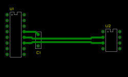
A quick example of how I would do the output, with as I said earlier pseudo diff pair routing. I could do with your full schematic including output filter to give a much better answer as their is a loop of high frequency noise that goes from the outputs and is shunted down to ground by the output filter.
As to splitting the digital and analogue sections, what software are you using?
Generaly most CAD software allows more than one connection code (route width), a basic starter is to have four separate codes:
GND, all ground connections
VCC, all power connections
DIG, all digital signal connections
ALG, all analogue signal connections
These can be displayed in different colours so when placing the components you can see by the rats nest and the different signal colours where the signals flow and change the layout to avoid digital and analogue signals crossing.
It will be easier to demonstrate this with an example layout hence a full schematic.
Grounding of Mixes Signal Systems
http://www.ti.com/lit/an/slyt499/slyt499.pdf
http://www.analog.com/static/import...gue/5467026043687049331665676350Grounding.pdf
Attachments
A list of some basic links I provide for PCB designer's just starting out that want some basic info....
All the usual subjects such as Henry Ott, Howard Johnson, Eric Bogatin are in there plus links to EMC guides. Now EMC is one area where a lot of DIYers get the wrong idea (comments such as EMC doesn't matter to DIY designs)...EMC and Signal Integrity are two sides of the same coin, and both are critical to a successful design...
Don't be put off by the quantity, just glance through a few, and use the rest as a reference. I do need to update this list when time permits...
Now if you want complex analogue digital grounding problems try a 50 channel phase array sonar")
All the usual subjects such as Henry Ott, Howard Johnson, Eric Bogatin are in there plus links to EMC guides. Now EMC is one area where a lot of DIYers get the wrong idea (comments such as EMC doesn't matter to DIY designs)...EMC and Signal Integrity are two sides of the same coin, and both are critical to a successful design...
Don't be put off by the quantity, just glance through a few, and use the rest as a reference. I do need to update this list when time permits...
Now if you want complex analogue digital grounding problems try a 50 channel phase array sonar
Attachments
Last edited:
Hi.
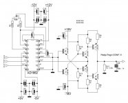
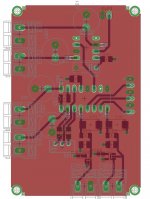
Im posting a dual layer pcb i designed some months ago for AD1862 with AD844 for i/v. Digital supplies have onboard regs (mic5207). I havent etched the boards mainly because i havent really studied how to implement logic ic's yet. Any comments are welcome
Im posting a dual layer pcb i designed some months ago for AD1862 with AD844 for i/v. Digital supplies have onboard regs (mic5207). I havent etched the boards mainly because i havent really studied how to implement logic ic's yet. Any comments are welcome
Attachments
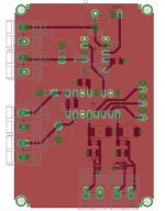
My only comment would be some vias very close to pads which may cause solder thieving.
I presume those are very small SMD (0402) caps next to the pins, cool, again watch for solder thieving due to the proximity of the pth hole, though if you do the AS1862 first it shouldn't be much of a problem...But may make soldering the chip cap a bit more problematic.
Also some thermal relief on the GND pads would help.
So my only caveat would be to just give these components a bit more room for soldering and move the vias out from the pads a little bit.
Other than that the analogue and digital is separated, the layout is neat and simple, job well done
That looks really neat! I see how you have managed to separate the digital and analog sections. Did you ever consider making a stereo dac board?
As for the glue logic. We don't really need to think about flip flops and shift registers anymore, because the I2SoverUSB receiver can output a compatible 20-bit "PCM" signal directly. With separate DL and DR lines.
If you compare with my layout suggestion, you can see that the digital lines and the +-5V supply have switched places. I think you got it right. A question to marce; how would you place "several decoupling caps strategically around the board"? That is if one were to use two 100 nF SMD caps for filtering on each of the digital supply lines. Henry Ott suggests spreading them out across the board.
Attachments
You don't, you have one contiguous ground plane.
A quick example of how I would do the output, with as I said earlier pseudo diff pair routing. I could do with your full schematic including output filter to give a much better answer as their is a loop of high frequency noise that goes from the outputs and is shunted down to ground by the output filter.
As to splitting the digital and analogue sections, what software are you using?
Generaly most CAD software allows more than one connection code (route width), a basic starter is to have four separate codes:
GND, all ground connections
VCC, all power connections
DIG, all digital signal connections
ALG, all analogue signal connections
These can be displayed in different colours so when placing the components you can see by the rats nest and the different signal colours where the signals flow and change the layout to avoid digital and analogue signals crossing.
It will be easier to demonstrate this with an example layout hence a full schematic.
I you use this pseudo diff pair routing, would you still connect it dac chip and the I/V stage to the same ground plane?
I use sPrint layout from Abacom. It doesn't support color coding of rubber bands unfortunately. Maybe I need to switch to Eagle.
I don't have a full schematic ready yet, but I will upload it when I do. I will probably be using Pedja Rogics discrete circuit. The only filtering will be a 330pF cap across the iv-resistor (1-2k). So the high frequency noise from this output stage will be looping back the dac ground?
Thanks for all the links! I have to admit that feels a bit overwhelming. I'll have a look at it. Seems there's a lot I need to learn.
Decoupling first, Henry Ott is talking more of boards with more components and pins, with BGA's etc, boards 100mm x 100mm can have a few hundred components and 5000+ pins, for this sort of design the caps you have will be adequate. Some boards with multiple gates switching can have instantaneous current demands in the 100A region, hence the importance of decoupling capacitors (if you want to fry your brain look up "simultaneous switching noise").
The pseudo balanced connections are used on some complex analogue digital boards where we want to avoid cross channel interference (think military headsets and communication) and probably a bit of overkill for this design, it also depends on the topology of the layout. if you are going direct into an op-amp as Skouliki has done above, both devices are on the same GND plane, you would join the AGND pin to this plane at the DAC, then run a signal from this pin to the op-amp - pin, as I have shown above, but do not connect this - pin to the GND plane (otherwise the current would travel through both). I will try and throw together an illustration as it is easier to follow. This is quite a specialised technique and I only use it on critical audio/analogue designs where ultimate signal fidelity and cross talk avoidance is required, generally just using the ground plane can suffice and people wont notice any difference.
The colour coding of the rubber bans isn't strictly necessary, but is a great help in visualising the rats nest, especially when you end up with a few thousand connections
Rather a lot of info, it is a generic list I give people who are going into professional PCB design, as on another forum one of the regular questions was "what do I need to know to do PCB design" and I got sick of giving the same answer so I just post that file, for hobby design probably overkill, for professional PCB design it is the basics.
Thank you guys for your kind words!
Those are 0402 caps indeed. I tried once to solder these things and it was a major pain but i succeeded- the trickiest part is to actually find them if they happen to slide or bounce out of my sight
I thought of creating thermal reliefs but if i understand correctly inductance is increased because of them.
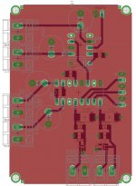
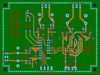
I made some attempts to create a stereo board but i couldnt get it right. Analog and digital was mixing up and i thought it would be better to create a mono board and stack two of them vertically. The stack could be a bit tall because im planning to stack two or three AD844's for I/V.
That usb to pcm thingie looks really interesting.
Those are 0402 caps indeed. I tried once to solder these things and it was a major pain but i succeeded- the trickiest part is to actually find them if they happen to slide or bounce out of my sight
I thought of creating thermal reliefs but if i understand correctly inductance is increased because of them.
I made some attempts to create a stereo board but i couldnt get it right. Analog and digital was mixing up and i thought it would be better to create a mono board and stack two of them vertically. The stack could be a bit tall because im planning to stack two or three AD844's for I/V.
That usb to pcm thingie looks really interesting.
I read this years ago when I doing HD video design. I STRONGLY recommend reading it. It will answer a lot of questions.
Analog Devices: Analog Dialogue: Ask The Applications Engineer - 12
G²
Analog Devices: Analog Dialogue: Ask The Applications Engineer - 12
G²
I made some attempts to create a stereo board but i couldnt get it right. Analog and digital was mixing up and i thought it would be better to create a mono board and stack two of them vertically.
Those were my thoughts exactly! I built a prototype with two dacs on one board, but I just couldn't get it right. One of the channels always ended up being really noisy.
I use very efficient loudspeakers, and at -0dB analog attenuation and the digital input set to -60 dB there's audible distortion when playing music. With a mono board I was able to use the MSB-trim to adjust this distortion away completely. So you might want to consider the MSB-trim. The right way to go is to play a -60dB test signal, hook the dac to a scope and adjust for minimum distortion.
Decoupling first, Henry Ott is talking more of boards with more components and pins, with BGA's etc, boards 100mm x 100mm can have a few hundred components and 5000+ pins, for this sort of design the caps you have will be adequate. Some boards with multiple gates switching can have instantaneous current demands in the 100A region, hence the importance of decoupling capacitors (if you want to fry your brain look up "simultaneous switching noise").
The pseudo balanced connections are used on some complex analogue digital boards where we want to avoid cross channel interference (think military headsets and communication) and probably a bit of overkill for this design, it also depends on the topology of the layout. if you are going direct into an op-amp as Skouliki has done above, both devices are on the same GND plane, you would join the AGND pin to this plane at the DAC, then run a signal from this pin to the op-amp - pin, as I have shown above, but do not connect this - pin to the GND plane (otherwise the current would travel through both). I will try and throw together an illustration as it is easier to follow. This is quite a specialised technique and I only use it on critical audio/analogue designs where ultimate signal fidelity and cross talk avoidance is required, generally just using the ground plane can suffice and people wont notice any difference.
The colour coding of the rubber bans isn't strictly necessary, but is a great help in visualising the rats nest, especially when you end up with a few thousand connections
Rather a lot of info, it is a generic list I give people who are going into professional PCB design, as on another forum one of the regular questions was "what do I need to know to do PCB design" and I got sick of giving the same answer so I just post that file, for hobby design probably overkill, for professional PCB design it is the basics.
Thanks for clarifying! This has turned out to be a very informative thread. I came here to learn about the analog and digital grounds, and ended up with a lot more.
So thanks for sharing your knowledge and giving constructive criticism. I'm gonna go make some schematics and layouts now, and I'll try to keep this thread alive until I have a finished product.
Those were my thoughts exactly! I built a prototype with two dacs on one board, but I just couldn't get it right. One of the channels always ended up being really noisy.
I use very efficient loudspeakers, and at -0dB analog attenuation and the digital input set to -60 dB there's audible distortion when playing music. With a mono board I was able to use the MSB-trim to adjust this distortion away completely. So you might want to consider the MSB-trim. The right way to go is to play a -60dB test signal, hook the dac to a scope and adjust for minimum distortion.
You are right. I thought at first to implement the MSB-trim but since my measuring equipment is limited to only a mediocre multimeter, i gave up that thought. I will try to squeeze the MSB-trim on the pcb. It will be usefull- someday i may get a scope
Very informative link stratus46. Thank you
Last edited:
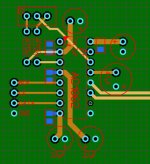
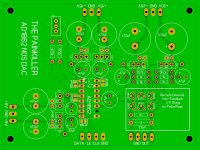
I implemented the trimm resistor and fixed the vias. I have a concern that the trimm resistor is close to the "digital" side of the board. Should i move it further away?
Don't know if it has any influence on sound quality. I'd have moved it closer to the edge of the board, and made it a trimmer with the adjustment screw on the side. Then you can trim even when the boards are stacked.
Don't know if it has any influence on sound quality. I'd have moved it closer to the edge of the board, and made it a trimmer with the adjustment screw on the side. Then you can trim even when the boards are stacked.
Havent thought of that. Great idea Painkiller
Ok, so here's my suggestion for a four layer PCB. Still using sPrint Layout. The output stage is only connected to the ground plane at the Agnd pin of the dac. 0805 caps for supply decoupling on the dac. Ground planes on top and bottom stitched together with vias around the edges. Any feedback on this?
Attachments
- Home
- Source & Line
- Digital Line Level
- AD1862 PCB layout