Does anybody have a circuit diagram for a Low Phase noise 100MHz Clock with CMOS 5V output levels for a Digital Audio project I’m working on?
Short-term jitter is very important – not worried about the longer-term frequency drift.
I’m looking for close-in sideband noise better then –135dBc /Hz at 10Hz with better then –160dBc /Hz at 10KHz!
As a side note, be aware that standard High Frequency Clock modules above say 25MHz use PLL multipliers, typically X4 (Normally the ICS501 from Integrated Circuit Systems). These have very poor short-term Phase Noise performance typically 100pS RMS Jitter.
The last discrete oscillator I designed (very poorly) was a complete pain – hopefully someone out there has something better to hand…
Any help very much appreciated!
JohnW said:Does anybody have a circuit diagram for a Low Phase noise 100MHz Clock with CMOS 5V output levels for a Digital Audio project I’m working on?
Short-term jitter is very important – not worried about the longer-term frequency drift.
I’m looking for close-in sideband noise better then –135dBc /Hz at 10Hz with better then –160dBc /Hz at 10KHz!
I would suggest reappraising the requirements for this part. I've helped design QAM-256 modulation equipment for the cable industry and the phase noise requirements you've listed are far stringent then required for that application.
A quick perusal of OCXO and VCXO type parts reviesl 10Hz offset phase noice in the -100dBc range...a far cry from -135.
Good luck.
Scott
Hi Scott,
Thanks for your reply, your right that the specification requirements are very high, but I’ve just checked the specs for the HP10811A/B 10MHz Quartz Crystal Oscillator (this is an OVEN unit), and they quote –120dBc /Hz at 10Hz and –160dBc/Hz @ 10KHz. This unit is not renowned for its short-term phase noise.
The fact that this is an oven unit has very little to do with its short-term stability (Phase Noise) – but more to do with its Longer-Term Frequency Stability.
As I’ve said earlier, “Off The Shelf” commercial grade Crystal Oscillators, VCXO’s and OCXO’s are more often then not, based on IC oscillator / PLL building blocks - and as a result have poor Phase Noise performance - as you also have discovered and highlighted.
Simple discrete designs (based on Butler or Colpitts oscillators), while not possessing the Long-Term Frequency Stability performance, can be designed to meet the short-term Phase-Noise – at a consumer price point ($2 to $3).
To design reliable oscillators at this frequency is a “Black Art” and requires a fair deal of experience and understanding – far more then I well ever claim to possess!
I recently came across a design Application Note from National Semiconductors for a clock driver for one of their ADC’s. I was a simple 3 or 4 transistor design (100MHz or 125MHz), but typically, I cannot find it now I need it… (No, I’m not confusing it with the Analog Devices AN-419, which has poorer performance @ –110dBc /Hz).
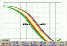
Below is the Phase Noise result of a commercial 90.3168MHz “Low Phase Noise” Crystal module. This unit was based on an ICS501 x4 PLL.
Still holding out hope…
Thanks for your reply, your right that the specification requirements are very high, but I’ve just checked the specs for the HP10811A/B 10MHz Quartz Crystal Oscillator (this is an OVEN unit), and they quote –120dBc /Hz at 10Hz and –160dBc/Hz @ 10KHz. This unit is not renowned for its short-term phase noise.
The fact that this is an oven unit has very little to do with its short-term stability (Phase Noise) – but more to do with its Longer-Term Frequency Stability.
As I’ve said earlier, “Off The Shelf” commercial grade Crystal Oscillators, VCXO’s and OCXO’s are more often then not, based on IC oscillator / PLL building blocks - and as a result have poor Phase Noise performance - as you also have discovered and highlighted.
Simple discrete designs (based on Butler or Colpitts oscillators), while not possessing the Long-Term Frequency Stability performance, can be designed to meet the short-term Phase-Noise – at a consumer price point ($2 to $3).
To design reliable oscillators at this frequency is a “Black Art” and requires a fair deal of experience and understanding – far more then I well ever claim to possess!
I recently came across a design Application Note from National Semiconductors for a clock driver for one of their ADC’s. I was a simple 3 or 4 transistor design (100MHz or 125MHz), but typically, I cannot find it now I need it… (No, I’m not confusing it with the Analog Devices AN-419, which has poorer performance @ –110dBc /Hz).
Below is the Phase Noise result of a commercial 90.3168MHz “Low Phase Noise” Crystal module. This unit was based on an ICS501 x4 PLL.
Still holding out hope…
Attachments
JohnW said:Does anybody have a circuit diagram for a Low Phase noise 100MHz Clock with CMOS 5V output levels for a Digital Audio project I’m working on?
Short-term jitter is very important – not worried about the longer-term frequency drift.
I’m looking for close-in sideband noise better then –135dBc /Hz at 10Hz with better then –160dBc /Hz at 10KHz!
Any help very much appreciated!
Hi Scott,
You will not find a 100MHz XO that can acheive -135dBc at
10Hz from carrier.
100MHz is not an optimal freq for low phase noise.
At 100MHz, even space qualified ultra low noise XO's won't
acheive -100dB at 10Hz. However they will acheive the
-160dBc noise floor at 10k
If you can drop to around 10MHz your specs are easily
acheivable and bettered... at a price.
Also, I'm not sure how these incredibly low phase noise
figures equate to sonics.
Perhaps better speak to Guido Tent one of the resident clock
experts.
Cheers,
Terry
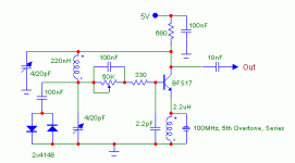
Long ago, I've built this XO (see image). Was used as a master oscillator for a DAC, and was operating near 98MHz. It performs quite well (sonically speaking), but never had the opportunity to measure the phase noise... No instruments  It needs to be followed by another stage for 5V output. Personally, I've used a MC710ELT21 ECL comp, as per Analog's AN419, but flavours can differ here. If by any chance you build a version, I'd sure be interested by the phase noise figures . And if the NS AN you're looking for comes handy, let us know
By the way, I know that Elso have a 100MHz XO he uses for asynchronous reclocking, but he'll sure be wandering around here
It needs to be followed by another stage for 5V output. Personally, I've used a MC710ELT21 ECL comp, as per Analog's AN419, but flavours can differ here. If by any chance you build a version, I'd sure be interested by the phase noise figures . And if the NS AN you're looking for comes handy, let us know By the way, I know that Elso have a 100MHz XO he uses for asynchronous reclocking, but he'll sure be wandering around here
Attachments
Thanks for replies.
First of all Pls. let me express my apologies to Scott if I’m wrong about being able to meet the Phase Noise requirements @ 100MHz with a crystal Oscillator.
Thanks to Cheff De Gaar, I will try his Oscillator design – when I can source the inductors.
Can anybody Pls. explain why it’s so hard to meet the Phase Noise requirements with a 100MHz Oscillator, and not with a 10MHz unit?
As an example, lets use the 10MHz HP10811D/E Opt 002 - which is guaranteed to be better then –133dBc /Hz @ 10Hz. Am I wrong it stating that the equation for Phase Noise scaling with frequency is: -
20Log (F2/F1)
So therefore a Super “100MHz HP10811D/E Opt 002” should have a Phase Noise at 10Hz offset of –113dBc / Hz?
Ok this figure is 22dB off my target, but its far better then most Low Phase Noise Oscillators modules I’ve found.
If a Crystal Oscillator cannot meet my target, what about LC or SAW Oscillators (not thinking about costs)?
Help - still tormented with Dynamic Range limitations due to Phase Noise!
JohnW said:Thanks for replies.
First of all Pls. let me express my apologies to Scott if I’m wrong about being able to meet the Phase Noise requirements @ 100MHz with a crystal Oscillator.
Thanks to Cheff De Gaar, I will try his Oscillator design – when I can source the inductors.
Can anybody Pls. explain why it’s so hard to meet the Phase Noise requirements with a 100MHz Oscillator, and not with a 10MHz unit?
As an example, lets use the 10MHz HP10811D/E Opt 002 - which is guaranteed to be better then –133dBc /Hz @ 10Hz. Am I wrong it stating that the equation for Phase Noise scaling with frequency is: -
20Log (F2/F1)
So therefore a Super “100MHz HP10811D/E Opt 002” should have a Phase Noise at 10Hz offset of –113dBc / Hz?
Ok this figure is 22dB off my target, but its far better then most Low Phase Noise Oscillators modules I’ve found.
If a Crystal Oscillator cannot meet my target, what about LC or SAW Oscillators (not thinking about costs)?
Help - still tormented with Dynamic Range limitations due to Phase Noise!
Sorry, my reply was to John not Scott.
John,
Why do you require such low phase noise? And what is
the application.
Cheers,
Terry
Hi Terry,
I’m evaluating and characterizing Digital Modulators for a project I’m working on.
ZETEX ZXCW8100/6100 1MHz HPWM, MCLK 768Fs, 120dB Dynamic Range
ZETEX ZXCW8100/6100 2MHz HPWM, MCLK 768Fs, 124dB Dynamic Range *
NSP6000 MCLK 2048Fs 101dB Dynamic Range
TI5015 MCLK 2048Fs, 111.5dB Dynamic Range *
Sony CXD9634 (M65817AFP) 117dB Dynamic Range MCLK 1024Fs *
All the Dynamic Range results are Awtd.
* Results limited by Master Clock Phase Noise
At the lower Master clock frequencies, it’s been much easier to Generate a Low Phase Noise Clock; this gives the Zetex and Sony modulators an advantage. Standard oscillator modules at these lower frequencies tend to be simple discrete based designs. These simple designs achieve very good Phase Noise results – unlike the higher frequency PLL multiplier designs.
Despite the ZETEX’s better Dynamic range with 1MHz HPWM (with optimal output stage) it suffers from many faults: -
Very poor noise floor modulation at higher output levels – up to 15dB!
Very poor Third Order 19KHz & 20KHz IMD products @ -63dB, compare this to the TI at –115dB under the same conditions!
Due to faults in its modulation scheme, places a very high demand on the output stage performance.
And above all, poor sonic quality
The TI scores wonderfully, despite it only have a PWM rate of 8Fs, Shame it doesn’t have an inbuilt SRC or Gain / Tone functions.
The Sony CXD9634 (M65817AFP), has better Dynamic Range performance then the TI @ 117dB, but poorer 3rd Order 19KHz & 20KHz IMD of about –105dB. However, it does have a SRC and Gain Controls – but no tone features.
I’ve just received first silicon of an 8fs modulator (I’m under NDA, so I cannot reveal names), that has a theoretically 140dB dynamic range – at least in the digital domain. The limiting factors will be the external circuits – where the PWM signal becomes “Analogue”. The single biggest limiting factor will be the 2048Fs Master Clock.
Re-latching of the PWM data and Clock Generation and Clock routing to these latches will be done “Off Chip” to give the best chances of evaluating the performance of the Digital modulator section – so the reason behind my hunt for a “commercially priced” Low Phase Noise 100MHz Clock source solution.
Reference
For those of you looking for a reference and further information on the design of this circuit, it can be found in Appendix B of Robert J. Matthys' book, "Crystal Oscillator Circuits", Revised Edition 1992, Krieger Publishing Company, ISBN 0-89464-552-8
James
CheffDeGaar said:Long ago, I've built this XO (see image).
For those of you looking for a reference and further information on the design of this circuit, it can be found in Appendix B of Robert J. Matthys' book, "Crystal Oscillator Circuits", Revised Edition 1992, Krieger Publishing Company, ISBN 0-89464-552-8
James
Whilst I don't have any circuits, the basics for low phase noise are : -
Maximum loaded Q, a 10dB increase in loaded Q gives 20dB improvement in phase noise.
An active device with the lowest corner frequency and lowest noise figure to help keep the 1/f noise increase minimal.
High impedance devices like FETs often work best.
Maintain a 90deg crossing angle between the device line and the load line for the oscillator, this minimises the potential for amplitude to phase modulation conversion.
Take the output of the oscillator through the crystal this uses the high-Q bandpass characteristics of the crystal (but don't allow this to affect the Q through the additional loading!)
This site may be useful: - http://www.wenzel.com/
Andy.
Re: Reference
Absolutely, and more exactly it's entitled "Emitter coupled XO". Mentionned as "outstanding" by Matthys, in terms of short term stability. I shamelessly borrowed this circuit from this thread. Very useful infos here.
Some infos of this kind on this post of the above mentionned thread.
nemestra said:
For those of you looking for a reference and further information on the design of this circuit, it can be found in Appendix B of Robert J. Matthys' book, "Crystal Oscillator Circuits", Revised Edition 1992, Krieger Publishing Company, ISBN 0-89464-552-8
James
Absolutely, and more exactly it's entitled "Emitter coupled XO". Mentionned as "outstanding" by Matthys, in terms of short term stability. I shamelessly borrowed this circuit from this thread.
Very useful infos here.ALW said:Whilst I don't have any circuits, the basics for low phase noise are : -
Maximum loaded Q, a 10dB increase in loaded Q gives 20dB improvement in phase noise.
An active device with the lowest corner frequency and lowest noise figure to help keep the 1/f noise increase minimal.
High impedance devices like FETs often work best.
Maintain a 90deg crossing angle between the device line and the load line for the oscillator, this minimises the potential for amplitude to phase modulation conversion.
Take the output of the oscillator through the crystal this uses the high-Q bandpass characteristics of the crystal (but don't allow this to affect the Q through the additional loading!)
This site may be useful: - http://www.wenzel.com/
Andy.
Some infos of this kind on this post of the above mentionned thread.
Thanks for the leads to Wenzel.com – one of the best sites on the Web for Phase Noise. After reading though the site, I can see that my 10Hz @ 100MHz target is not going to be met – once again my apologies to Scott!
Also, thanks for leads to Robert J. Matthys book, "Crystal Oscillator Circuits" – sent my $50 + P&P today, hopefully this should be winging its way to me - by good old snail mail.
After researching the Wenzel Site, I’m guessing I will be very lucky to meet -110dBc / Hz at 10Hz, although I should be able to meet my 10KHz target.
Does anybody have any idea of the Phase Noise performance of the newer CMOS logic families such as the VHC & UHS TinyLogic Gates? The best of the older families was the AC series with about –140dBc / Hz @ 10KHz! Also any ideas of the Phase Noise performance of PECL?
I’ve just started to use LVDS – and have found this to be poor – worst then UHS. LVDS is very sensitive to fast edges coupling into it – such as CMOS logic lines. Have found it very hard to find any real Phase Noise Specs on LVDS, the only papers I have found are on LVDS in Communication systems where they can tolerate up to 20% jitter before the error rates creep too high! NS AN977 “LVDS signal quality”
Pls. keep the 100MHz clock ideas coming in; I’m going to try using a Zetex FMMT617 (High Current – low fT). I’ve used this on amplifier input stages and found it to have VERY low 1/f noise at low currents (possibly due to its very low Re value). Not sure how its large Cobo will effect the performance – maybe it might work better in “Grounded Base” oscillator circuits?
Zetex have new GEN5 devices, which might work better…
JohnW said:Does anybody have any idea of the Phase Noise performance of the newer CMOS logic families such as the VHC & UHS TinyLogic Gates? The best of the older families was the AC series with about –140dBc / Hz @ 10KHz! Also any ideas of the Phase Noise performance of PECL?
Not phase noise figures, but their close cousin in the time domain, jitter. See the following interesting numbers
http://www.diyaudio.com/forums/showthread.php?postid=293292#post293292
Hope you like the book, though not many hard phase noise numbers in it.
James
I’ve been looking at the Specs of the MC10ELT21, the Motorola Data sheet states a Fmax of 100MHz and a RMS jitter value of 35pS which seems very poor for an ECL device.
In the Analog Devices Data sheet AN-419, I wonder how much of the 110dBc / Hz phase noise is due to the MC10ELT21. It well not help that the MC10ELT21 is operating 25% faster then the Data Sheet Fmax – you can be sure that its Jitter performance will be even worst!
Does anybody have a good cheap level buffer / Amp to use in place of the MC10ELT21?
Hi JohnW,
Do you think it is really necesarry to have such a low noise master oscillator? TAS5015 divides master clock by 256 to obtain 384kHz PWM frequency. So master oscillator jitter is 256 times or 48dB lower at PWM output. I think there will be far greater contribution to jitter from internal frequency division in TAS5015 and especially output stage.
Here is quote from Analog AN-419 tu support my view
Best regards,
Jaka Racman
BTW, what is the best comercially available can oscillator that you have found so far? I have found this .
Do you think it is really necesarry to have such a low noise master oscillator? TAS5015 divides master clock by 256 to obtain 384kHz PWM frequency. So master oscillator jitter is 256 times or 48dB lower at PWM output. I think there will be far greater contribution to jitter from internal frequency division in TAS5015 and especially output stage.
Here is quote from Analog AN-419 tu support my view
Reference oscillator phase noise, in conjunction with the residual phase noise of the AD9850, constitutes the total phase noise of the DDS output signal. Residual phase noise of the AD9850 at 1 kHz offset from a 5 MHz carrier with a 125 MHz reference clock is –134 dBc. DDS, by virtue of its frequency division characteristic, will reduce the reference oscillator’s phase noise contribution by 20 LOG (Output Frequency/Reference Frequency). For example, the Butler oscillator’s phase noise contribution to the AD9850 output signal is reduced from a typical –110 dBc to –138 dBc when clocking at 125 MHz and outputting 5 MHz. As the DDS output frequency becomes a greater percentage of the reference oscillator frequency, the oscillator’s contribution to the DDS output phase noise will increase.
Best regards,
Jaka Racman
BTW, what is the best comercially available can oscillator that you have found so far? I have found this .
Hi Jaka,
The best XO I’ve found are from WWW.WENZEL.COM (sorry not sure how to post links).
I’ve also come across the unit you’ve found, but its Close-in Phase Noise is not that good.
True the Phase Noise reduces by 20LOG N, but does this still hold true for the DC component - where the noise is “Bounced of” and reflected directly into the Audio Band?
I’m not claiming to fully understand modulation theory here, but from my Lab work I observe a very stronger correlation between Carrier Phase Noise (Spurie levels) which then are demodulated into the audio band at an all most a 1:1 level.
I’m I missing something here?
Just thinking - how can you tell if the noise you see “Offset” from the carrier – is not in fact noise modulated UP from DC? (after all 1/f noise is, predominately a LF issue). This would then explain why it is so strongly demodulated in the AF band – I believe this to be the real issue.
It's just been one of those things "You see all the time", take for granted, and never try to expain!
JohnW said:
Yes, Wenzel is where I quoted the original
10MHz Vs 100MHz figures from. They appear
as good as it gets, I believe.
Unfortunately even their low spec XO's (which beat most other peoples high spec ones) are very expensive. Their ultra low noise XO's can run into thousands of dollars

Start saving
WRT to discrete designs posted here using low noise BJT's,
I beleive there are Toshiba devices available
that are 0.5nV/rt Hz, you could parallel a few of these
up maybe?
Cheers,
Terry
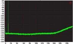
Here’s an FFT (Ref. to 0dB) of the TI5015 @ -60dB. I believe you can see the effects of the poor Close-in Phase Noise of the 98MHz Clock. Awtd DR 111.5dB
It might also be that TI has played around with their Pole’s & Zero’s of their Noise shaper to achieve more Feedback at higher Frequencies – as sensible thing to do. If so, this might explain the unusual “shaped” Noise Floor, and how they have achieved such good 19KHz & 20KHz IMD results. With normal FB structures you end up with massive amounts of correction at DC, and very little at 20KHz.
Even if TI have played with their NS Pole’s & Zero’s, I still believe the LF noise floor to be to high.
Attachments
- Status
- This old topic is closed. If you want to reopen this topic, contact a moderator using the "Report Post" button.
- Home
- Source & Line
- Digital Source
- Circuit wanted for a Low Phase noise 100MHz Clock